Original Link: https://www.anandtech.com/show/6170/four-multigpu-z77-boards-from-280350-plx-pex-8747-featuring-gigabyte-asrock-ecs-and-evga
Four Multi-GPU Z77 Boards from $280-$350 - PLX PEX 8747 featuring Gigabyte, ASRock, ECS and EVGA
by Ian Cutress on August 22, 2012 9:15 AM ESTWith only sixteen PCIe 3.0 lanes available on a Z77 motherboard paired with an Ivy Bridge CPU, when we get to three or four-way GPU solutions these GPUs are itching to get more bandwidth. The Z77 specification limits us to three GPUs anyway, at x8/x4/x4. For some extra cost on the motherboard, we can add in a PLX PEX 8747 chip that effectively increases our PCIe 3.0 lane count, giving 32 PCIe 3.0 lanes overall. Today we discuss this technology, and look at four motherboards on sale today that utilize this PLX chip - the Gigabyte G1.Sniper 3, the ASRock Z77 Extreme9, the ECS Z77H2-AX and the EVGA Z77 FTW.
Multi-GPU on Z77
Aiming for users for 3-way and 4-way GPU setups is aiming for a very niche sub-section of an enthusiast crowd. Here we are pinpointing those that have the hard cash to create a very nice system, capable of powering several large monitors at high resolution for fast paced and detailed gaming. Many of these setups are bespoke, specifically designed in modded cases, and a good number use water-cooling to get around the generation of heat. Let us not forget the power draw, with multiple GPU setups requiring significant power supplies or even a dual power supply solution. It gets even worse if everything is overclocked as well.
These users often keep up to date with the latest and greatest hardware. No processor, no graphics card and no chipset is too new for them. If any of our enthusiasts here were asked about which platform would be best for a multi-GPU setup, we would respond with X79 and Sandy Bridge-E, should money be no object. Even for high throughput users, such as scientific simulators or video editing - Sandy Bridge-E holds all the performance. There is one thing Sandy Bridge-E lacks though - PCIe bandwidth.
With the majority of X79 stuck in PCIe 2.0 land, we start to hit bottlenecks transferring data between memory and GPU. Our limit is 8 GB/s for a full sixteen lane PCIe 2.0 port. If we jump into Z77 and Ivy Bridge, we have PCIe 3.0. For a full sixteen lane PCIe 3.0 port, we have double the bandwidth at 16 GB/s.
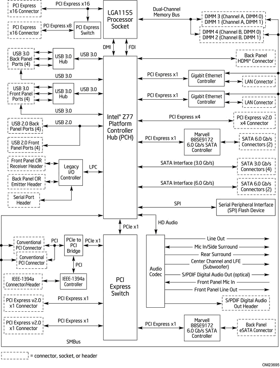
The other issue is lanes - X79 and SBE have 40 PCIe 2.0 lanes to distribute, giving x16/x8/x8/x8 in a four-way GPU scenario. Even with double the bandwidth per lane of PCIe 3.0, Z77 and Ivy Bridge can only play around with sixteen lanes in total, as shown by the chipset diagram:
The Z77 specification states that these lanes can be split in any of the following ways:
| PCIe Layout Comparison Chart | |||||
| Configuration | GPUs | GPU 1 | GPU 2 | GPU 3 | GPU 4 |
| 1 | 1 | 16x PCIe 3.0 | - | - | - |
| 2 | 2 | 8x PCIe 3.0 | 8x PCIe 3.0 | - | - |
| 3 | 2 | 16x PCIe 3.0 | 4x PCIe 2.0 | - | - |
| 4 | 3 | 8x PCIe 3.0 | 4x PCIe 3.0 | 4x PCIe 3.0 | - |
| 5 | 3 | 8x PCIe 3.0 | 8x PCIe 3.0 | 4x PCIe 2.0 | - |
| 6 | 4 | 8x PCIe 3.0 | 4x PCIe 3.0 | 4x PCIe 3.0 | 4x PCIe 2.0 |
For many of these setups, motherboard manufacturers can also choose to direct four of the PCIe 2.0 lanes from the chipset to also aid with CrossFire scenarios (SLI is not certified in this configuration). The downside of this comes from the limited bandwidth of the PCIe 2.0 lanes, which have half the bandwidth of the PCIe 3.0 lanes, but there is also added latency of navigating data through the chipset rather than across the PCIe bus.
For mini-ITX solutions, we will see the one GPU scenario. For many microATX solutions, one of the dual GPU scenarios will dominate. In full ATX mode, manufacturers have all the configurations listed above to choose from. Luckily, here at AnandTech, we have reviewed the majority of the configurations (1, 2, 4 and 5) in the table above in order to provide comparison points.
Back in the days of X58 and P55, when PCIe 2.0 dominated the landscape, certain motherboards contained a special chip called an NF200. This was a PCIe switch that allowed the motherboard to double its quota of PCIe 2.0 lanes from 16 to 32, which could then be arranged appropriately. The downsides of using this chip were that it added cost to the board, it drew more power, and there was some slight processing overhead from using it. However, if it allowed full bandwidth to a second GPU and increased FPS by 40%, then a small ~1-3% deficit on top was not worried about.
Fast forward a few years and we have another chip on the market, this time doing exactly the same thing with PCIe 3.0 lanes. This chip is the PEX 8747, designed by the company PLX (you may see it referred to as a PLX PEX 8747 or a PLX 8747). It offers PCI Express switching capability, giving motherboard manufacturers 32 PCIe 3.0 lanes to play with. This allows the following combinations:
| PCIe Layout Comparison Chart | ||||||
| Configuration | GPUs | PEX 8747 | GPU 1 | GPU 2 | GPU 3 | GPU 4 |
| 7 | 1 | Y | 16x PCIe 3.0 | - | - | - |
| 8 | 2 | Y | 16x PCIe 3.0 | 16x PCIe 3.0 | - | - |
| 9 | 3 | Y | 16x PCIe 3.0 | 16x PCIe 3.0 | 4x PCIe 2.0 | - |
| 10 | 3 | Y | 16x PCIe 3.0 | 8x PCIe 3.0 | 8x PCIe 3.0 | - |
| 11 | 4 | Y | 16x PCIe 3.0 | 8x PCIe 3.0 | 8x PCIe 3.0 | 4x PCIe 2.0 |
| 12 | 4 | Y | 8x PCIe 3.0 | 8x PCIe 3.0 | 8x PCIe 3.0 | 8x PCIe 3.0 |
In reality, configuration 8 may be selected on micro-ATX sized boards, and configurations 10 and 12 will be applied to ATX boards. The rest are not likely to be on a product in market.
Now we have a direct competitor to the 40 PCIe 2.0 lanes of X79, in that we have 32 PCIe 3.0 lanes - equivalent to 64 PCIe 2.0 lanes (or x16/x16/x16/x16 on PCIe 2.0).
How Does a PCI Express Switch (like the PEX 8747) Work
The key confusion surrounding devices such as the PEX 8747 is that no matter how many lanes there are to be seen by the CPU, the CPU still only has 16 lanes for data travel. Data is always limited by this bottleneck, so how do we get more lanes? I see many posts of forums saying 'well it multiplies it by two', but that is not a proper answer.
When searching for data on the PEX 8747, or the NF200, there is a lot of forum talk and not a lot of technical information. The PLX website hosts some high-level information, and low-level technical data is under NDA. Thus, what we write here is from what I have discussed with technical minded colleagues, and potentially does not represent the true actions of the PEX 8747.
The heart of the PLX chip is how it manages the data between the CPU and the PCIe slots. It does this through multiplexing, or the art of dealing with multiple signals wanting to travel through one point. We already deal with multiplexing on some motherboards with respect to the power delivery. Here are some basic examples of multiplexing:
Signal multiplexing: Combining multiple analogue signals into a single signal. This signal can then be optimized for high speed travel. The single signal is then de-multiplexed (de-muxed) at the other end to extract the original data. This is performed on a large scale with telecommunications.
Time-division multiplexing: Instead of installing several fast connects between two points that have multiple users at each end, one line is installed and this line switches between each of the pairs of users such that the signal is not inadvertently disrupted. This gif from the Wikipedia helps describe this scenario:
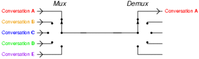
So what does the PLX chip do on a motherboard? Our best reasoning is that it acts as a data multiplexer with a buffer that organizes a first in, first out (FIFO) data policy for the connected GPUs. Let us take the simplest case, where the PLX chip is powering two GPUs, both at ‘x16’. The GPUs are both connected to 16 lanes each to the PLX chip.
The PLX chip, in hardware, allows the CPU and memory to access the physical addresses of both GPUs. Data is sent to the first GPU only at the bandwidth of 16 lanes. The PLX chip recognizes this, and diverts all the data to the first GPU. The CPU then sends data from memory to the second GPU, and the PLX changes all the lanes to work with the second GPU.
Now let us take the situation where data is needed to be sent to each GPU asynchronously (or at the same time). The CPU can only send this data to the PLX at the bandwidth of 16 lanes, perhaps either weighted to the master/first GPU, or divided equally (or proportionally how the PLX tells the CPU at the hardware level). The PLX chip will then divert the correct proportion of lanes to each GPU. If one GPU requires less bandwidth, then more lanes are diverted to the other GPU.
This ultimately means that in the two-card scenario, at peak throughput, we are still limited to x8/x8. However, in the situation when only one GPU needs the data, it can assign all 16 lanes to that GPU. If the data is traveling upstream from the GPU to the CPU, the PLX can fill its buffer at full x16 speed from each GPU, and at the same time send as much of the data up to the CPU in a continuous stream at x16, rather than switching between the GPUs which could add latency.
This is advantageous – without a PLX chip, the GPUs have a fixed lane count that is modified only by a simple switch when other cards are added. This means in a normal x8/x8 setup that if data is needed by one GPU, the bandwidth is limited to those eight lanes at maximum.
With all this data transference (and that should data be going the other way to memory then the PLX chip will have to have a buffer in order to prevent data loss) the PEX introduces a latency to the process. This is a combination of the extra routing and the action of the PEX to adjust ‘on-the-fly’ as required. According to the PLX documentation, this is in the region of 100 nanoseconds and is combined with large packet memory.
Back in the days of the NF200, we experienced a 1-3% overhead in like-for-like comparisons in many of our game testing. The PEX 8747 chip attempts to promise a reduction in this overhead, especially as it only comes into play in extreme circumstances. The situation is more complex in different circumstances (x16/x8/x8).
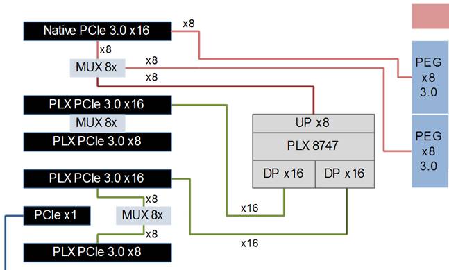
Take for example one of the boards we will review - the Gigabyte G1.Sniper 3. Gigabyte on this board chooses to route all the 16 PCIe 3.0 lanes from the CPU into the PLX PEX 8747 chip, and distribute them accordingly:

From this diagram alone, we can see that the PEX 8747 chip directs 16 PCIe 3.0 lanes to one PCIe slot and 16 to another slot. Should cards be entered in the PCIe slots underneath these primary cards, then the sixteen lanes will be split by the switch into x8/x8 accordingly. The PEX 8747 then decides how to distribute the bandwidth given these lane options and prioritized data through multiplexing and the FIFO buffer contained on chip. The downside of this comes with a single GPU setup, whereby the added latency and routing caused by the PLX chip can reduce single card performance.
One other option with lane routing is to split the lanes from the CPU. As we will see on the EVGA Z77 FTW in a later review, eight PCIe 3.0 lanes can be directed to the first PCIe slot, and the other eight PCIe 3.0 lanes can be sent to the PLX PEX 8747 chip. This solution uses the 32 lane output to populate other PCIe slots in the following manner:
Many thanks to EVGA for the diagram
In this lineup, the CPU provides eight PCIe 3.0 lanes to the first PCIe slot, and the other eight lanes to a multiplexer that either directs the lanes to the first PCIe, or the PEX 8747 chip. The eight upstream lanes in the PLX chip are organized into 32 downstream lanes, which are sent 16 each to the second PCIe x16 slot and the fourth PCIe x16 slot. Those 16 lanes are each shared with the slot directly below.
What this means is that the second, third and fourth PCIe lanes, even if they are rated ‘x16’, are limited by the eight lanes upstream from the PLX. While the chip can handle multiple inputs and outputs, that eight lane restriction to the CPU could become an issue. EVGA tell us that their configuration gives better single and dual GPU performance than other manufacturers. Most GPU communication is between GPUs through SLI fingers which is not effected by the 8 lanes upstream, and the PLX chip is clever enough to shut down parts it doesn’t need depending on the configuration, saving power.
This allows for the following configurations:
| PCIe Layout Comparison Chart | ||||||
| Configuration | GPUs | PEX 8747 | GPU 1 | GPU 2 | GPU 3 | GPU 4 |
| 13 | 1 | Y |
16x 8x from CPU 8x via MUX |
- | - | - |
| 14 | 2 | Y | 8x from CPU | - | 16x from PLX | - |
| 15 | 2 | Y | - | 16x from PLX | 16x from PLX | - |
| 16 | 3 | Y | 8x from CPU | 16x from PLX | 16x from PLX | - |
| 17 | 4 | Y | 8x from CPU | 16x from PLX | 8x from PLX | 8x from PLX |
The differences between configurations 14 and 15 should be explained. While configuration 15 has a total of 16 lanes per GPU on average, if we refer back to the diagram above, these GPUs are limited to the CPU by the 8 lanes upstream from the PLX. By placing the GPUs in configuration 14, we are minimizing latency to the CPU for the first GPU while giving each GPU a maximum of 8 lanes each direct to the CPU (even if they are through the PLX for the second GPU).
Yes, using a PLX PEX 8747 chip makes understanding how the lanes work on a motherboard very confusing. No longer can these motherboards really represent what is going on by quoting electrical lane connections. But alas, that is the only way to report them in marketing and PR.
If a manufacturer really wanted to push the limits, they could add multiple PEX 8747 chips to the motherboard. We will see this on the ASRock X79 Extreme11 in a future review, as they take 32 lanes from the Sandy Bridge-E GPU and use the PLX chip to produce 64 lanes, giving a peak of x16/x16/x16/x16 bandwidth. (The other eight lanes seem to be directed to an LSI SAS RAID chip - we will investigate this when we review the motherboard.)
But onward to the motherboard reviews – the first up is the Gigabyte G1.Sniper 3.
Gigabyte G1.Sniper 3 Overview
Based on our Gigabyte Z77X-UD5H review, if we extrapolate up to the G1.Sniper 3, then we should be in for a real treat. In our testing, the Gigabyte G1.Sniper 3 did definitely throw up a few surprises, and given the feature set, is one of the more competitive price versus functionality motherboards in this combined review.
Visually on its own, the G1.Sniper 3 has a good balance on green and black on the motherboard, however this may me a lost aesthetic inside a case with a lot of PCIe devices inside it – the intended market for this product. The G1.Sniper 3 aims at gamers, specifically those who want an Ivy Bridge platform setup as well as two or more GPUs. With the PLX chip, it also performs at peak x8/x8/x8/x8 GPU setups, wired such that in dual usage it retains x16/x16.
The G1.Sniper 3 currently retails for $280 on Newegg, and for the money there is a lot of added functionality that people will use. We have one Killer NIC for gaming, an Intel NIC for networking features, a Creative CA0132 audio chip, an mSATA port, a total of ten USB 3.0 ports, all four video outputs and a PS/2 port all wrapped up in an E-ATX form factor (one inch wider than ATX).
The package really shines when we open the box, which contains a WiFi PCIe x1 card, dual antenna, eight SATA cables, a USB 3.0 front panel and rigid SLI connectors. There is a little question mark over the choice to include a WiFi card, given the system already has increased cost due to the dual Killer/Intel NIC scenario.
Performance also gives us an extra point to think about. Some Z77 manufacturers are taking advantage of what has been called ‘MultiCore Enhancement’, where instead of running an i7-3770K CPU at 39x/39x/38x/37x during 1/2/3/4 threaded load, the CPU will run 39x/39x/39x/39x. Gigabyte does this on their main channel boards, the UD3H and UD5H. They go a step further on the G1.Sniper 3, by providing a default overclock at any load to 40x (it will idle at 16x). This gives the G1.Sniper 3, out of the box, essentially a clean sweep in all our CPU tests. It sometimes translates in our GPU testing as well. But without an overclock, the G1.Sniper 3 is the first board to come with a ‘better than the highest Turbo multiplier’ overclock.
Visual Inspection
The first thing to notice about the Gigabyte G1.Sniper 3 is the size of the board. It is one of two boards in this roundup that uses the E-ATX form factor, which means that there is an extra inch of width to the motherboard. This allows Gigabyte to place a larger chipset heatsink if it wanted, more controllers, or an improved layout. Real estate is often a premium on a high end product, so jumping up to the next motherboard size can make sense given most gamers this product is aimed at will have full sized ATX cases.
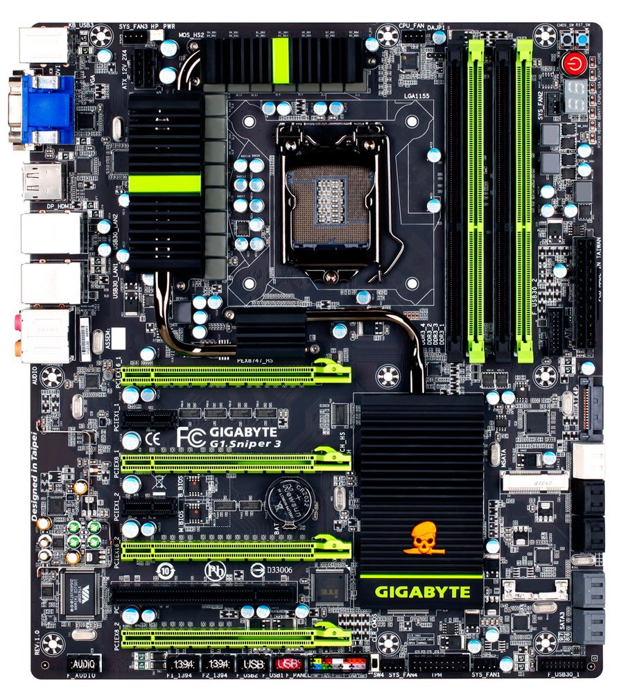
The green and black livery is accented by a gold skull and knife on the chipset heatsink. All the heatsinks are solid and finned, designed to take air in one direction each to aid cooling, and are also connected by heatpipes in order to distribute the heat away from the warm areas. The socket area is surrounded on three sides by these heatsinks, which measure ~30mm up from the PCB at the highest point, though they are set away from the Intel minimum designated socket area. The socket area has access to three fan headers nearby – a system 4-pin fan header to the top left near the 8-pin CPU power connector, a CPU 4-pin fan header to the right of the top heatsink, and a second 4-pin system fan header next to the two-digit debug button on the right.
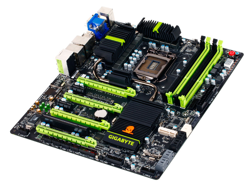
Along the right hand side of this 6-layer PCB (there is a number on the reverse bottom of all GB boards that tells us this) are a large number of connectors that Gigabyte have added with the extra PCB space we have. At the top is a trio of power/reset/ClearCMOS buttons, with the power button being big and red. I would like Gigabyte in the future to make the reset button distinct as well, such that enthusiasts will not accidentally be clearing their BIOSes instead of resetting their systems.
Underneath this is a two-digit debug display, useful for diagnosing POST issues and a series of voltage read points if users are willing to solder on their own meters. Beside the 24-pin ATX power supply is a USB 3.0 header, powered by a nearby VIA chip. This header is in the perfect place for the USB 3.0 front panel included in the box - the VIA chip also powers the USB 3.0 header at the bottom right of the board. Beside the SATA ports we have a SATA power connector, for supplying more power to multi-GPU setups on board. I prefer having this type of connector here, as opposed to the molex or 6-pin connectors we sometimes find just above the PCIe slots.
Gigabyte have thankfully split their SATA ports by color, making them easier to understand – the white ports are the chipset SATA 6 Gbps ports, the black are the chipset SATA 3 Gbps ports, and the grey are the SATA 6 Gbps powered by two Marvell controllers. The mSATA port just beside the normal SATA ports shares lanes with one of the chipset SATA 3 Gbps ports, so it is something to bear in mind if you are using an mSATA device.
The bottom of the board on most motherboards is often populated with USB 2.0 headers (as the Z77 chipset allows a lot of them) or power/reset buttons, but typically Gigabyte takes a different approach. Here Gigabyte are using a VIA VT6308P chip (the really big one at the bottom left) to power two IEEE1394 headers, should anyone require these ports. Alongside these are two USB 2.0 headers, the front panel header section, a BIOS switch (to go between the two onboard BIOSes), a pair of fan headers, and a TPM module. As we have discussed in previous Gigabyte reviews, Gigabyte like to add a TPM module as it is often requested by their business partners. How useful it may be on the top of their range gaming board, I am not sure.
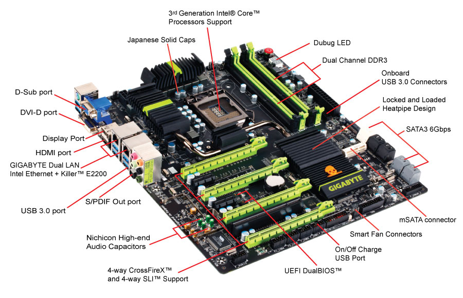
The PCIe ports are what all these motherboards reviewed today are all about, and Gigabyte point out which ones are for GPUs with the bright green color. By using the PLX PEX 8747 chip underneath the middle heatsink, the PCIe lanes are split such that:
One GPU: x16/-/-/-
Two GPUs: x16/-/x16/-
Three GPUs: x16/-/x8/x8* or x8/x8/x16/-
Four GPUs: x8/x8/x8/x8*
*These configurations use a GPU in the bottom PCIe slot. If the GPU is dual slot, it could restrict some of the space available for these bottom headers, such as my power connectors shown here:

The audio on the G1.Sniper 3 is one point which sets this board apart from the others in this review – Gigabyte have decided to use a Creative CA0132 chip, separated in its own area of the PCB with an EM shield to help reduce interference. The chip is also accented with audio-specific Nichicon capacitors, which are reputed to be better than the standard audio caps used.

The rear IO panel is covered in a myriad of features – from left to right we have a combination PS/2 port, two USB 3.0 ports, D-Sub, DVI-D, DisplayPort, HDMI, four more USB 3.0 ports, an Intel 82579V NIC, a Qualcomm Atheros Killer NIC (2201-B), audio jacks and a S/PDIF output. While Gigabyte has included all the video outputs, legacy is partly in the mind with D-Sub and PS/2 here. There is no USB 2.0, which makes life difficult as only some of the USB 3.0 ports work on first install of an OS – two of the six should work as they are based off the chipset. However, here is another point – Gigabyte have two VIA USB 3.0 controllers on board for 8 USB 3.0 ports, and the chipset should provide four more to make twelve in total. But Gigabyte only uses two from the chipset, as per their chipset diagram.
Board Features
| Gigabyte G1.Sniper 3 | |
| Price | Link |
| Size | ATX |
| CPU Interface | LGA-1155 |
| Chipset | Intel Z77 |
| Memory Slots |
Four DIMMs, Supporting up to 32GB DDR3 1066-2666 MHz, Non-ECC |
| Video Outputs |
D-Sub DVI-D HDMI DisplayPort |
| Onboard LAN |
Qualcomm Atheros Killer E2200 Intel GbE |
| Onboard Audio | Creative CA0132 |
| Expansion Slots |
2 x PCIe 3.0 x16 (x8 when slots underneath are occupied) 2 x PCIe 3.0 x8 2 x PCIe 2.0 x1 1 x PCI |
| Onboard SATA/RAID |
2 x SATA 6 Gbps (Intel), Supports RAID 0, 1, 5, 10 4 x SATA 3 Gbps (Intel), Supports RAID 0, 1, 5, 10 1 x mSATA 3Gbps (Intel) shared with SATA2_5 4 x SATA 6 Gbps (Marvell 9172), Supports RAID 0, 1 |
| USB |
2 x USB 3.0 (Intel) [2 back panel] 8 x USB 3.0 (VIA VL810) [4 back panel, 4 onboard] 4 x USB 2.0 (Intel) [4 onboard] |
| Onboard |
6 x SATA 6 Gbps 4 x SATA 3 Gbps 1 x mSATA 3 Gbps 5 x Fan Headers 2 x USB 3.0 Headers 2 x USB 2.0 Headers 2 x IEEE1394 Headers Power/Reset Buttons ClearCMOS Button BIOS Switch Voltage Measurement Points TPM Header |
| Power Connectors |
1 x 24-pin ATX Power Connector 1 x 8-pin CPU Power Connector 1 x SATA Power Connector (for PCIe) |
| Fan Headers |
1 x CPU 4 x SYS |
| IO Panel |
1 x PS/2 Combination Port 6 x USB 3.0 1 x D-Sub 1 x DVI-D 1 x HDMI 1 x DisplayPort 2 x Network Ports (Intel, Killer) 1 x Optical S/PDIF Output Audio Jacks |
| Warranty Period | 3 Years |
| Product Page | Link |
The main features of the Gigabyte G1.Sniper 3 are in terms of functionality against price. For $280 of your hard earned cash, we get dual NIC (one Intel, one Killer), ten USB 3.0 ports, 10 SATA ports, 4-way SLI and CrossfireX through a PLX PEX 8747 chip, any video output for the iGPU wanted, a TPM module, and improved audio through the Creative CA0132 chip. For legacy, we have a PS/2, D-Sub, a PCI port and IEEE1394 headers.
Gigabyte G1.Sniper 3 BIOS
The BIOS of a system is a measure of how much effort a manufacturer likes to put into every aspect of their design. A good BIOS reflects commitment and perseverance to producing a good product versus just getting one out there into the market. There is no use ever having one BIOS engineer on staff, even if a company only produces one motherboard. The design of the BIOS has to come from multiple sources, and a creative piece has to come out which improves the user experience and the functionality, rather than being merely another check point on the list.
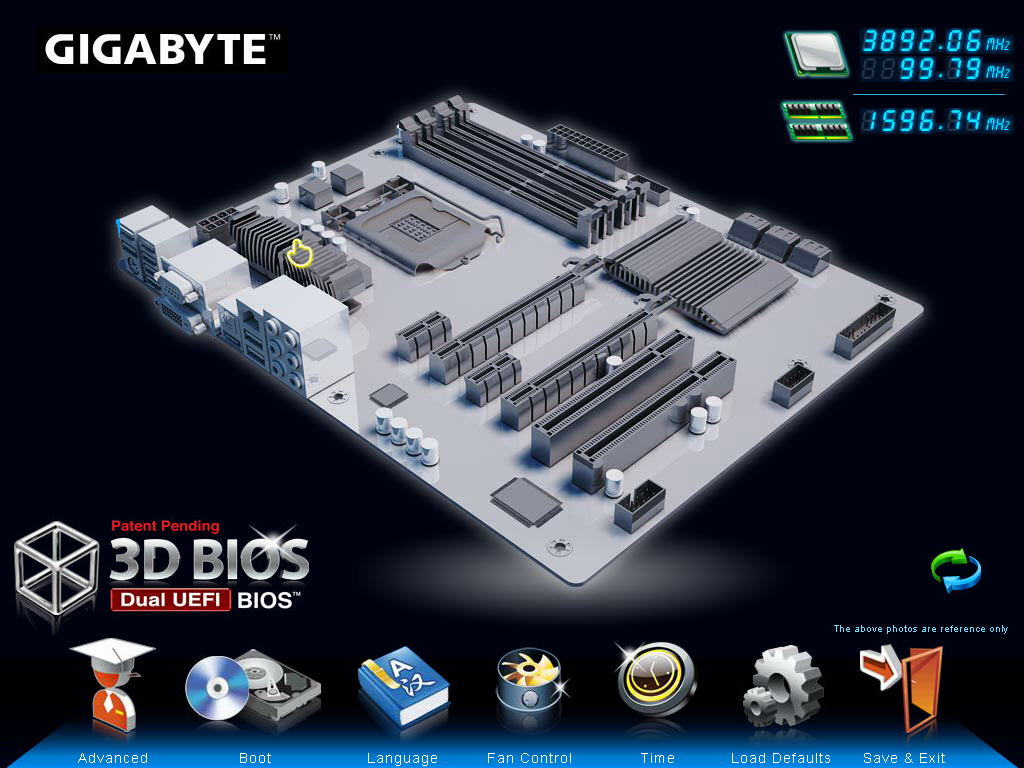
So here we are with the Gigabyte G1.Sniper 3 BIOS, which is essentially an identical replica of the BIOS we saw on the Z77X-UD5H reviewed recently, despite this motherboard being part of the gaming range of Gigabyte motherboards. Our opening screen represents Gigabyte’s ‘3D’ mode screen, showcasing a representative motherboard on the screen. Different parts of the image are clickable, which present menus for the specific areas of the motherboard.
While this is a good way to introduce users to the BIOS, it does leave several questions, as we raised with the Z77X-UD5H. We have no text declaring which motherboard is being used (if the board is in a case), the BIOS version or the CPU. The motherboard point is the most poignant, as Gigabyte use a generic motherboard image in their 3D BIOS rather than one specific to the motherboard at hand. Other manufacturers also include information such as the temperatures, the memory count, memory speeds, voltages, and fan speeds on the front page – for Gigabyte’s model, we have to click through to find this information.
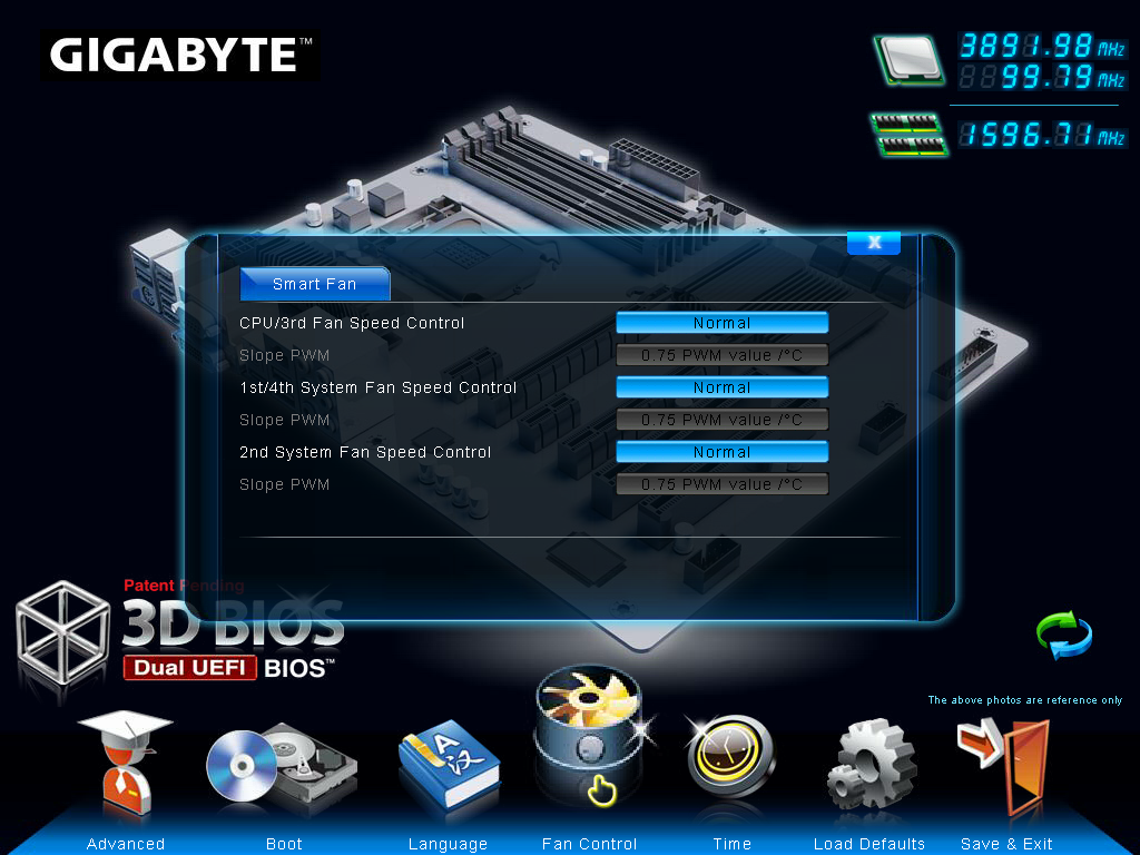
Users can also adjust the fan controls here, by clocking on the ‘Fan Control’ option on the menu at the bottom. As mentioned in previous Gigabyte reviews, the fan controls on their boards are not the best by any stretch, as the options available to users consist of choosing a fan ramp in terms of PWM values per degree. We would prefer options which relate to % fan speeds to temperature, with options to select initial and final temperatures and speeds such that the ramp was calculated automatically by the system. In our review of Biostar Z77 motherboards, we at least got an automatic testing option to tell us which PWM values should be set, even if they are an arbitrary scale for the majority of users should they wish to delve in and understand what is being said.
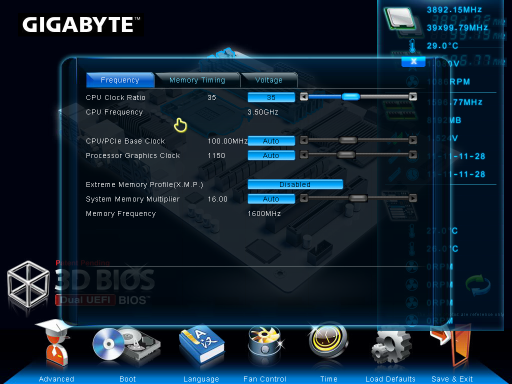
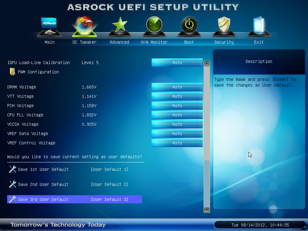
The main section of the Gigabyte BIOS is found in the Advanced option on the bottom row. This pulls up a more vintage style BIOS scenario, easily navigable by both the mouse and the keyboard. The first screen is labeled ‘MIT’, and we also get information regarding the BIOS version, the BCLK, memory size, temperatures and voltages here. The MIT screen also has a ‘Current Status’ option which gives a more detailed overview of some of the more important numbers relating to the hardware in the system.
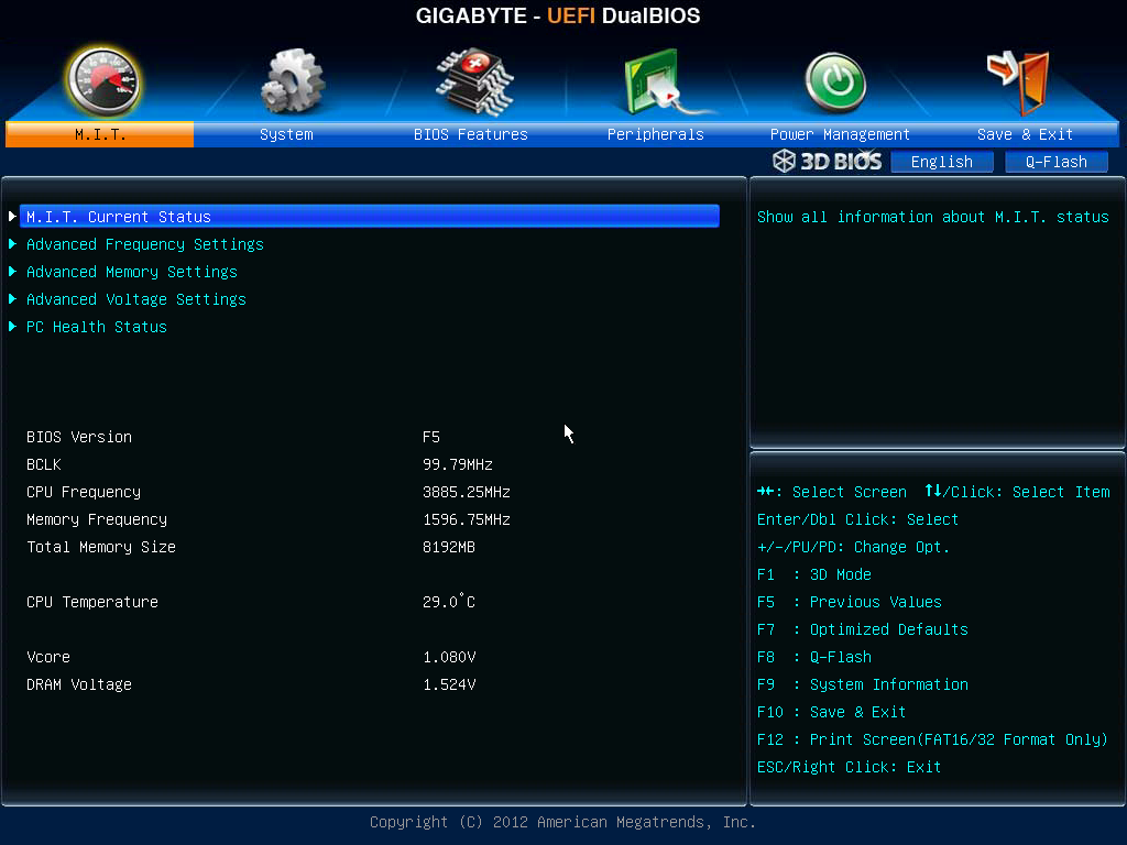
The overclocking options are found in a series of three menus from the MIT screen. To adjust the CPU and memory frequencies, these options are found in the ‘Advanced Frequency Settings’ menu. In the ‘Advanced Memory Settings’ screen, the memory frequency is again adjustable, but also the subtimings are adjustable here. For voltages of the CPU or the memory, or other voltages in the system and Load Line Calibration settings, these are found in the ‘Advanced Voltage Settings’ menu. It is a little frustrating having to navigate between several menus at once to pick the CPU speed, and then set the appropriate voltage and LLC. I hope that in the future Gigabyte will make an all-in-one menu and have the appropriate options visible to see.
.png)
.png)
.png)
.png)
.png)
Elsewhere in the BIOS are the fan settings in a different menu format, as well as boot order selection, advanced peripheral management, and the BIOS flash utility.


Gigabyte G1.Sniper 3 Software
Much like the BIOS in the G1.Sniper 3 is essentially identical to that found in the Z77X-UD5H, there is not much difference in the software either. We still have the main stables of the software – EasyTune6 for monitoring and overclocking, @BIOS for updating the BIOS and 3D BIOS to adjust LLC settings and the power delivery on the fly. Due to some of the extra feature adjustments on the G1.Sniper 3 over the UD5H though, we also have software to manage the Qualcomm Atheros Killer Network controller, as well as the Creative audio chip on board.
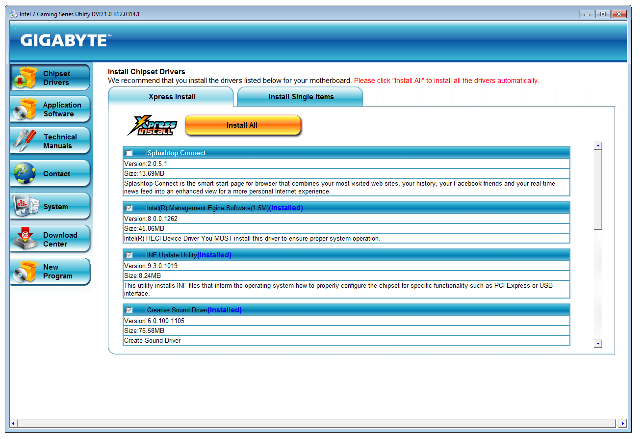
For installation of the software and drivers, the install CD that comes with the motherboard is simple to use – a one button click will install all the drivers and most of the software, including those needed for extra controllers and EasyTune6. 3D BIOS and software to enable 3TB hard drives is not installed by default however – these can be manually selected via the options menu. One other feature that we have not covered before, Gigabyte TweakLauncher, has to be downloaded from the website to be installed. This ‘new’ software is described below. After we finished testing the motherboard, Gigabyte released new software called ‘USB Blocker’ designed to restrict unwanted USB devices. We will be covering this software in a later review, however it will be available for the G1.Sniper 3.
EasyTune6
EasyTune 6 is Gigabyte’s attempt to bring together a lot of the functionality that the software should do in one package. Through ET6, we can perform automatic overclocking or manual overclocking, gather information regarding the system and the CPU being used, adjust the fan settings, or monitor the hardware voltages and temperatures.
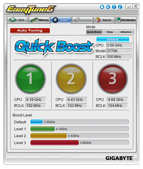
The first menu of ET6 takes us to the Tuner menu, which offers three level of overclocks (as shown above) as well as an ‘Auto Tuning’ option. The effect of these buttons is described in our overclocking section for this motherboard. Under the ‘Easy’ and ‘Advance’ options in the top right of the Tuner tab, we can explore the multiplier and voltage adjustments that ET6 allows:
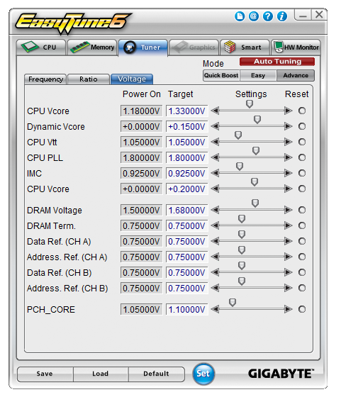
The main take-home point of ET6, apart from the fact that it is starting to look a little dated as it has not changed in at least 18 months, is that the fan controls are awkward compared to those provided by other manufacturers.
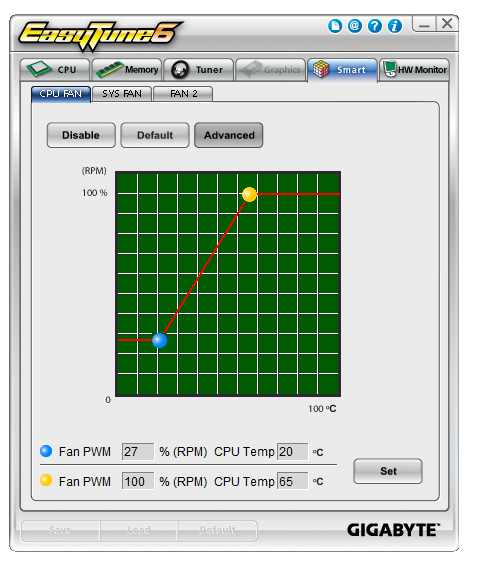
Users can set the CPU fan, the System fans, or the second series of fans as part of three different series each with their own ramp from a low speed to a high speed. These fan controls are easier to digest than those found in the BIOS, but Gigabyte needs to invest a bit more into their fan controllers and also the software that comes with controlling them.
It is also worth pointing out that ET6 still has the issue plaguing our Deferred Procedure Call testing, which determines how smoothly the processor goes through requests. Due to the monitoring software of ET6, every few seconds it causes the DPC to rise to 20 times its normal value. This can have serious effects in audio processing, introducing offsets of a couple of milliseconds. This situation can be avoided by turning off the ET6 software.
Qualcomm Atheros Killer Network Manager
As the Gigabyte G1.Sniper 3 comes with a Killer NIC onboard, there is also software designed to help manage this functionality. The Killer NIC is designed to prioritize certain kinds of traffic over others as well as reduce CPU usage, such that playing video games either at a LAN or on the internet is not disturbed by the network interface. This system is a combination of hardware and software, and the software allows for that priority configuration to be manipulated.
Users will notice a new icon in their task bar when the software is installed, which will bring up the following ‘Overview’ screen of the software:
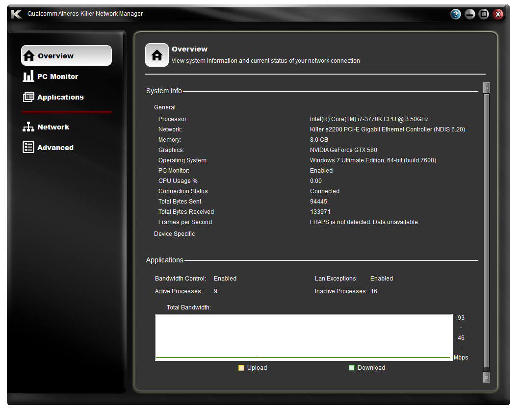
The software gives a good overview of the system being used, but the crucial options are found in the applications menu.
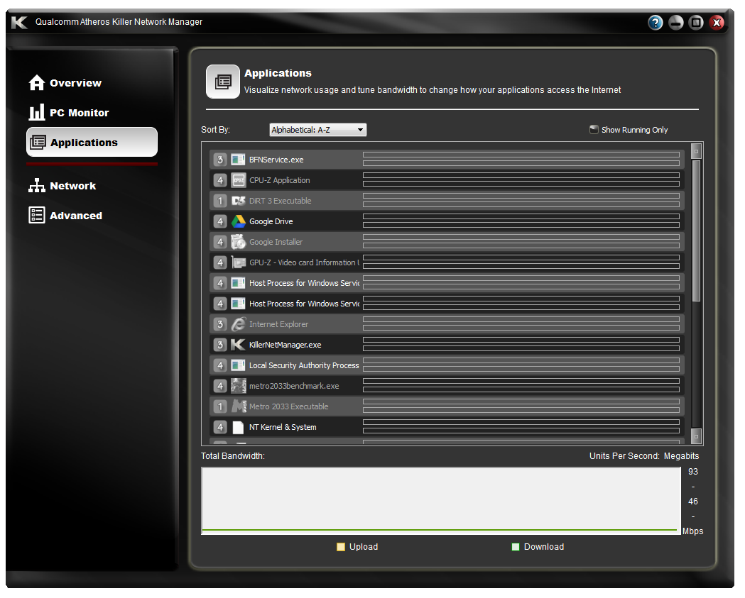
This allows users to see all the programs that request network services, and then give them a rating to indicate which ones have priority. For most gamers, this puts the game and any VOIP at the top priority, and everything else at the lowest. If the lowest priority programs request more networking resources when the priority programs require them, then the low priority requests are throttled. Users can also monitor the data through the network port though this tool.
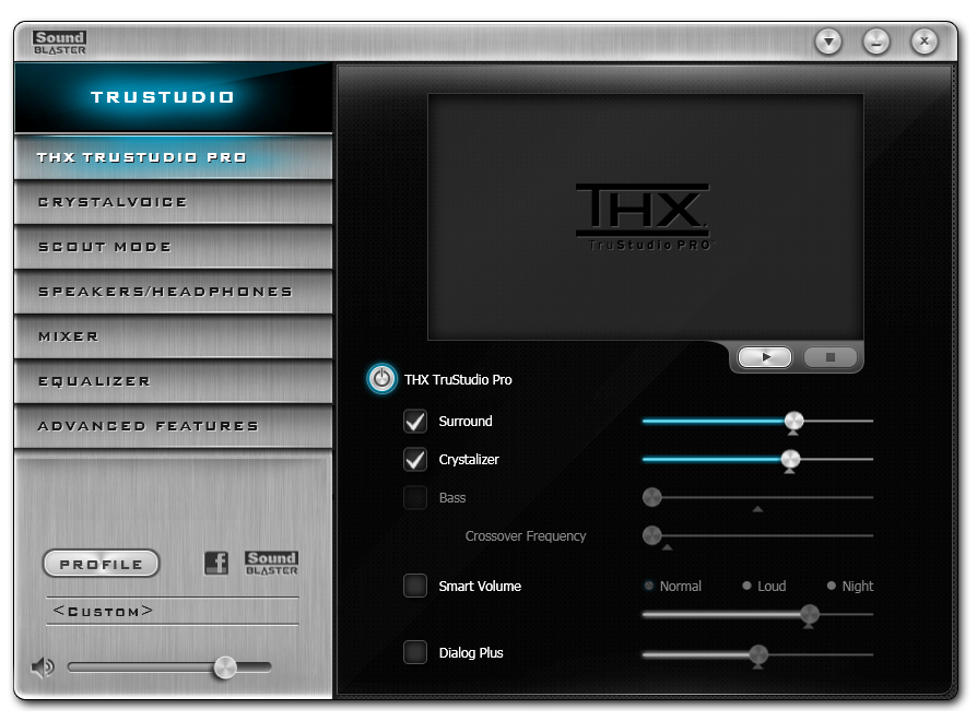
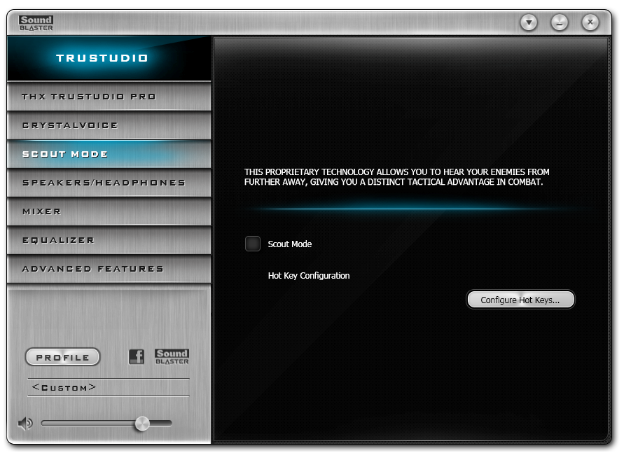
SoundBlaster THX TruStudio
Similar to the software management of the Killer NIC, the Creative audio chip on board has its own set of software utilities to manage the sound delivery on the motherboard. The software comes in the form of SoundBlaster THX TruStudio, and offers customization of all the audio ports in terms to an equalizer, setup, and enhanced voice controls. As part of this package, there is also proprietary post-audio processing technology to enhance audio related to in-game footsteps, to help determine when that enemy is creeping up behind you.
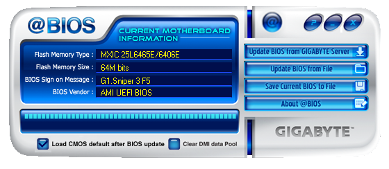
@BIOS
Users have two options to update the BIOS on a Gigabyte motherboard – if you have access to the internet via another computer and a USB stick, the BIOS can be updated through the BIOS itself and the Q-Flash utility. If that is not available (or the new BIOS is sufficiently different such that Q-Flash does not recognize the new BIOS), then in the operating system @BIOS can be used. The @BIOS system can check the Gigabyte servers for the latest BIOS for the motherboard and download it appropriately.
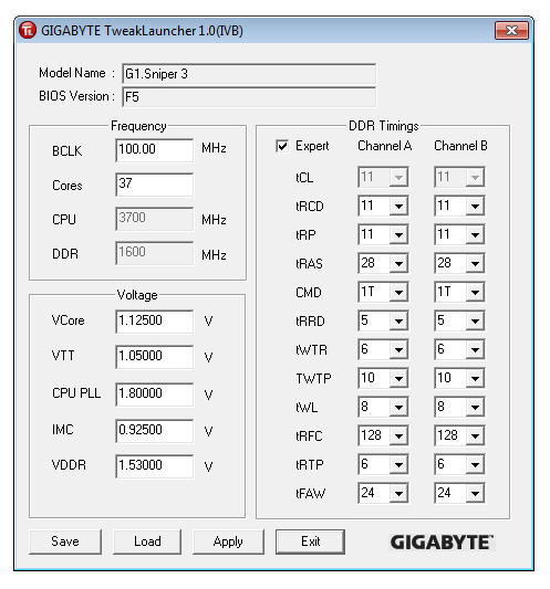
Gigabyte TweakLauncher (GBTL)
One relatively new bit of software to be released alongside Z77 motherboards is the Gigabyte TweakLauncher. This software is designed for competitive overclocking rather than any other overclocking, as it takes the entire GUI out of the overclock options in ET6 and gives the user the bare basics to give on-the-fly adjustments. This software is not available on the CD, but only through a download on the Gigabyte website.


Gigabyte G1.Sniper 3 In The Box
Gigabyte gives the user a very dichotomous relationship depending on the motherboard you buy. At the low end of the spectrum, the cheaper boards come with little else apart from a pair of SATA cables, an IO shield and a driver CD. At the higher end, such as the UD5/UD5H models and above, Gigabyte lays it on a little thicker with more cables, SLI rigid connectors, and possibly much more. So with the G1.Sniper 3 being above the UD5H, we expect a good deal in the box!
Rear IO Shield
Driver CD
User Manual
3-way SLI Rigid Connector
4-way SLI Rigid Connector
Eight SATA Cables
x1 PCIe Dual Band WiFi Card
Two WiFi Antenna
eSATA + Power Bracket
SATA Power Cables
Internal USB Cable
USB 3.0 Front Bracket
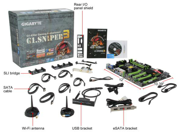
Gigabyte clearly does lay it on very think with the G1.Sniper 3, much to the joy of users everywhere. The usefulness of the WiFi card could perhaps be questionable as this is a board aimed at 4-way GPU users, though 3-way GPU users can take advantage of the spare space with that WiFi card and the eSATA bracket. So many SATA cables in the box are nice, as well as that USB 3.0 bracket and the SLI connectors.
Voltage Readings
After my first publication of OCCT voltage readings, a few readers responded with a more in-depth reasoning behind some of the results we were seeing. With this in mind, I would like to re-describe what we are doing with this test, and how it comes about.
Much of what an enthusiast overclocker does is monitor CPU temperature and voltage. Whatever settings a user places in the BIOS or OS is at the mercy of the motherboard - in terms of actually setting the values and reporting the values back. As an enthusiast, we have to rely on what readings we get back, and hope that motherboard manufacturers are being honest with their readings.
Take CPU voltage. What we as a user see in CPU-Z or OCCT is a time-averaged value that hides voltage ripple (if any) for power delivery. It is very easy for a motherboard manufacturer to hide this value, or to disregard slight deviations and report a constant value to the user. The CPU voltage reading can be taken at a variety of places on the power plane, which can vary between motherboards and manufacturers, meaning that each reading is essentially not comparable with the other. Nevertheless, as an enthusiast, we will constantly compare value A with value B.
Whether or not I can achieve 4.7 GHz with 1.175 volts on a particular board is inconsequential - your motherboard may perhaps produce the same result with a reading at 1.200 volts. The only way to test the actual value is with consistent methodology is via an oscilloscope connected to similar points on each board. This may sound like taking an OCCT reading is therefore redundant.
However, motherboards have settings relating to load line calibration. As load is applied to the CPU, the voltage across the processor decreases (VDroop). Load Line calibration essentially attempts to control this level of droop, by increasing voltage when voltage drops are detected away from a fixed value. Manufacturers have different ideas on how to modify LLC with respect to load, or whether the level of modification should be controlled by the user. Some manufacturers offer the option at a variety of levels, such that overclockers can be sure of the applied setting (even if it increases peak voltage, as explained by AnandTech in 2007).
By doing a full load OCCT test, we are essentially determining both how aggressive the motherboard is reporting the CPU voltage under load and how aggressive load line calibration is performing (from the point of view of the user without an oscilloscope or DVM). If someone has one of the motherboards we have tested and you have a different one, variations in load voltage should describe the offset you may require for overclock comparisons.
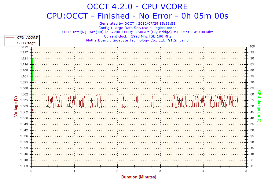
At stock, the G1.Sniper 3 showed that the voltage recorded by OCCT jumps around with a very large granularity – 0.10 volts or so. This is rather surprising – going back to the previous Gigabyte boards we have tested, we all got straight lines under the assumption that the values were being manipulated from the sensor to the operating system. If the case is that the granularity of that reporting is this large (rather than 0.02 volts on most other boards), then we have to wonder why this is the case.
We also looked at the OCCT readings when overclocked:
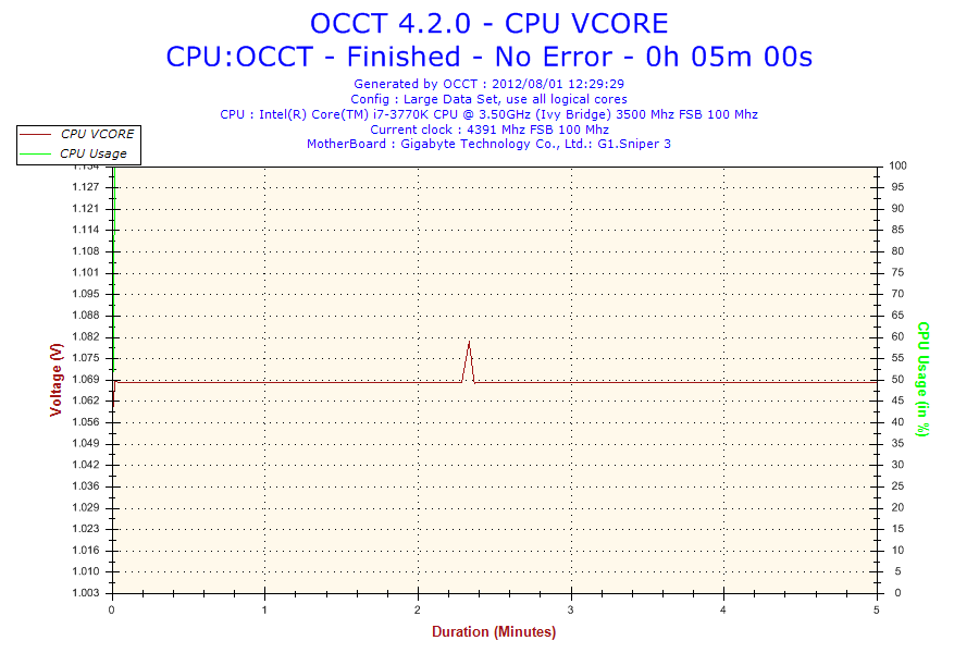
With our overclocked results (1.100 volts set in BIOS, also showing 1.068 volts in CPU-Z) we do indeed get a straight line. This could suggest that when the voltage is fixed in the BIOS by the user, the CPU load line configuration has more of a fixed gradient, compared to when it is set to Automatic (as shown above).
| Reported Load Voltage / V | |
| ASRock Fatal1ty Z77 Professional | 0.956 |
| ASRock Z77 Extreme4 | 1.050-1.058 |
| ASRock Z77 Extreme6 | 1.040-1.048 |
| ASRock Z77 Extreme9 | 1.016-1.024 |
| ASUS P8Z77-V Deluxe | 1.085 |
| ASUS P8Z77-V Pro | 1.090 |
| ASUS P8Z77-V Premium | 1.088 |
| Biostar TZ77XE4 | 1.036 |
| ECS Z77H2-AX | 1.048 |
| EVGA Z77 FTW | 0.698-0.706 |
| Gigabyte Z77X-UD5H | 1.067 |
| Gigabyte Z77X-UD3H | 1.067 |
| Gigabyte G1.Sniper 3 | 1.068-1.078 |
| MSI Z77A-GD65 | 1.020 |
Gigabyte G1.Sniper 3 Overclocking
Note: Ivy Bridge does not overclock like Sandy Bridge. For a detailed report on the effect of voltage on Ivy Bridge (and thus temperatures and power draw), please read Undervolting and Overclocking on Ivy Bridge.
Experience with Gigabyte G1.Sniper 3
Overclocking on the G1.Sniper 3 was a lot like the experiences we had with the Z77X-UD5H. Automatic overclocking had its issues depending on the memory kit used, whereas manual overclocking was easy to do and hit some good speeds.
Automatic overclocking is performed through the EasyTune6 software, and offers three levels depending on how adventurous a user you are. There is also an additional option called ‘Auto Tuning’, which uses a stress test program in order to find a good overclock given a users cooling and case situation.
Manual overclocking was performed entirely in the BIOS. Gigabyte still needs to refine this part of the overclocking procedure, as CPU voltages, speeds and load line calibration settings all in different menus (with up to four button presses to get between them). However, given the maturity of the 3D BIOS now, it was relatively quick and painless to navigate between them, if a bit slower than optimal for an enthusiastic well trained overclocker.
Methodology:
Our standard overclocking methodology is as follows. We select the automatic overclock options and test for stability with PovRay and OCCT to simulate high-end workloads. These stability tests aim to catch any immediate causes for memory or CPU errors.
For manual overclocks, based on the information gathered from previous testing, starts off at a nominal voltage and CPU multiplier, and the multiplier is increased until the stability tests are failed. The CPU voltage is increased gradually until the stability tests are passed, and the process repeated until the motherboard reduces the multiplier automatically (due to safety protocol) or the CPU temperature reaches a stupidly high level (100ºC+).
Our test bed is not in a case, which should push overclocks higher with fresher (cooler) air. We also are using Intel's All-in-one Liquid Cooler with its stock fan. This is a 120mm radiator liquid cooler, designed to mimic a medium-to-high end air cooler.
Automatic Overclock:
Using Gigabyte’s EasyTune6 software in the operating system, we applied the various overclock options it presents. These are in the form of three levels, each more aggressive than the last. The final option is an Auto Tuning, which applies a stress test to the CPU and gradually raises the voltages and CPU speed until a maximum given the cooling and the quality of the CPU is reached.
For the three EasyTune6 levels, the overclock is easy to understand – a new multiplier and BCLK is applied to achieve the relevant speed, and a voltage offset is used to keep it stable. The memory is also adjusted, to one strap below XMP. This is so the memory is not pushed above XMP due to the BCLK adjustment.
The issue we found with the ET6 overclock levels is the memory adjustment – the memory kit we use for our testing is very sensitive to adjustments, and would not work with any of the ET6 levels but did work at XMP. However a slower kit from Patriot did work with EasyTune on some of the levels.
Here are our results:
At Level 1, ET6 gave the CPU a 41x multiplier and 102.3 MHz BCLK, to give 4194.3 MHz total. A +0.110 volt offset on the CPU was also applied, as well as a memory adjustment to XMP minus one strap. However, this setting gave constant memory errors during PovRay.
At Level 2, ET6 gave the CPU a 43x multiplier and 103.3 MHz BCLK, to give 4441.9 MHz total. A +0.150 volt offset on the CPU was also applied, as well as a memory adjustment to XMP minus one strap. This was stable and gave peak temperatures of 85°C during PovRay and 89°C during OCCT.
At Level 3, ET6 gave the CPU a 45x multiplier and a 103.3 MHz BCLK, to give 4693.5 MHz total. A +0.150 volt offset on the CPU was also applied, as well as a memory adjustment to XMP minus one strap. This was stable and gave peak temperatures of 98°C during PovRay and 102°C during OCCT.
The Auto Tuning option resulted in giving the CPU a 47x multiplier and a 104.3 MHz BCLK, to give 4916 MHz total. The normal turbo bin procedure was also applied, giving 47x/47x/46x/45x for 1/2/3/4 threaded load, meaning 4707 MHz at full load. This setting showed 1.200 volts at load, and gave 90°C during OCCT but memory errors during PovRay.
Manual Overclock:
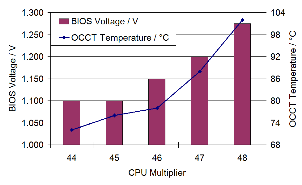
With our manual overclocking, we very early switched CPU Load Line Calibration to Extreme to improve stability and remove VDroop. On an LLC setting of automatic and a fixed CPU voltage of 1.100 volts, in the OS at load this dropped down to 1.068 volts. Changing LLC to extreme gave an OS reading of 1.104 volts, which usually results in a little extra temperature but improved stability all around. Here are our results:
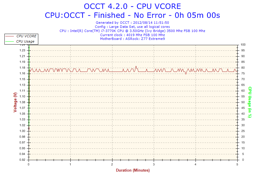
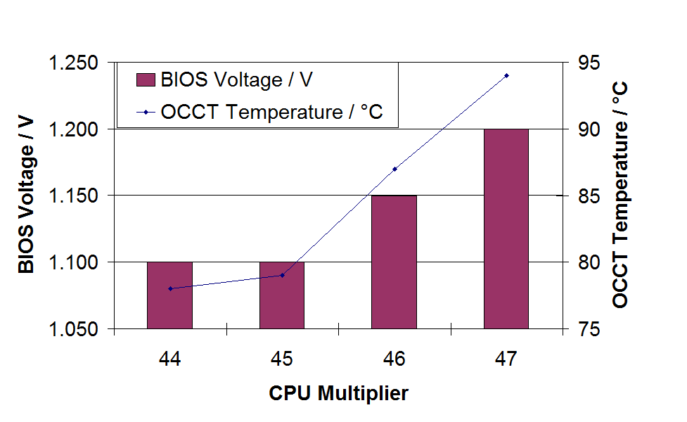
Starting at 44x multiplier and 1.100 volts, the system was stable with LLC on automatic and showed an OS load voltage of 1.068 volts. This gave peak temperatures of 69°C during PovRay and 72°C during OCCT.
The 45x multiplier was stable at 1.100 volts, but with the CPU LLC set to Extreme. This showed an OS load voltage of 1.104 volts. This also gave peak temperatures of 74°C during PovRay and 76°C during OCCT.
The 46x multiplier was stable at a minimum of 1.150 volts, with LLC set to Extreme and an OS load voltage of 1.152 volts. This gave peak temperatures of 79°C during PovRay and 78°C during OCCT.
The 47x multiplier was stable at a minimum of 1.200 volts, with LLC set to Extreme and an OS load voltage of 1.200 volts. This gave peak temperatures of 85°C during PovRay and 88°C during OCCT.
The 48x multiplier was stable at a minimum of 1.275 volts, with LLC set to Extreme and an OS load voltage of 1.272 volts. This gave peak temperatures of 97°C during PovRay and 102°C during OCCT.
Understandably we did not try higher speeds or voltages due to the load temperatures already being reached.
With this multi-board review, it is clear that a combination of performance and functionality paired with a low price will win the day. So in comes ASRock’s entry, in the form of the Z77 Extreme9. The Z77 Extreme9 boasts dual NIC (Broadcom), 10 SATA ports, 12 USB 3.0 ports, onboard WiFi with dual transmission/receivers, and six fan headers for $350. Having reviewed several ASRock Z77 motherboards so far, we are hoping that ASRock have stepped up the game for what is their high end Z77 model.
ASRock Z77 Extreme9 Overview
Unfortunately, the ASRock Z77 Extreme9 falls foul from the first test. Back when I reviewed the Z77 Extreme6, ASRock were frustrated that their motherboards were falling behind ASUS and Gigabyte due ASRock’s lack of MultiCore Enhancement (MCE). ASRock were preparing BIOSes which enabled this feature, and offered me a preview BIOS for the Z77 Extreme6 which was not available for public release. My policy is to only use BIOSes that are available on public release, and as I was not prepared to re-review the Extreme6 with a new beta-BIOS, I informed ASRock when I would be reviewing the Z77 Extreme9, giving them a date to get the BIOS for the Extreme9 configured in time.
To clarify my position regarding BIOS revisions – I can receive boards at any point of their release cycle, from before the chipset release to the very latest revision. The later boards obviously have an advantage with model design and BIOS efficiency, and the early boards may stuffer from issues with the beta BIOSes I receive. This means that when I place a motherboard on my test bench, I will automatically update to the latest publicly available BIOS online. I am not interested in beta BIOSes – if the public cannot access it, then it is not relevant to the consumer advice these reviews are supposed to represent. From time to time, motherboard manufacturers will release a public BIOS during my testing – as testing a board takes a good 25-30 hours (repeating IO, testing software, multiple GPU configurations) I cannot scrap several days of testing on a whim otherwise no results may ever be shown. As such, the moment I place the board on the test bed and update the BIOS, it is that configuration I am locked into (barring any crippling issues that prevent me from testing). If a manufacturer wishes me to add a note to my review regarding a proposed BIOS to be release with changes, I am more than happy to do so.
Thus when I started testing the ASRock Z77 Extreme9 slightly after the date I quoted to ASRock and updated to the latest public BIOS, I was expecting MultiCore Enhancement to be an option and a default setting in the BIOS, given their previous frustration. However, no such luck. The 1.40 BIOS features a variation of MCE for non-K processors, to allow them to overclock slightly, but nothing for the i7-3770K I am using in my testing.
Despite this, MCE is not an issue if a user intends to overclock the motherboard. The ASRock Z77 Extreme9, while it doesn’t perform like ASUS and Gigabyte in multithreaded benchmarks, does overclock well, and provides a good number of automatic overclock options in the BIOS should a user have sufficient cooling.
One feature that ASRock seem to have fixed is related to certain memory kits applying XMP. Previously I have had issues with my DDR3-2400 9-11-11 kit on ASRock Z77 motherboards, requiring extra VTT voltage and still fading in and out with stability. No such issues on the Z77 Extreme9, which took my XMP profile first time with perfect stability. The ASRock Z77 Extreme9 does feature a digital PWM, in the sense that some PWM features are now unlocked in the BIOS and available for adjustment.
ASRock has strong competition from Gigabyte, which will ultimately be their downfall – the Gigabyte is much more price competitive, has better features onboard, and performs better in our benchmark suite. ASRock can take pride by giving a user a lot of SATA and USB 3.0 ports (10 and 12 respectively), as well as offering dual NIC that support Teaming, and an integrated WiFi card in a mPCIe slot rather than the x1 card the Gigabyte offers. However, the ASRock Z77 Extreme9 lacks anything similar to the Killer NIC and the upgraded audio offered by the Gigabyte G1. Sniper3.
The ASRock Z77 Extreme9 is a good board with important features and certainly caters for the IO heavy user. But the competition is mightily aggressive in their strategy, which has perhaps caught ASRock out.
Visual Inspection
No matter which way you slice it, the ASRock Z77 Extreme9 looks like a very busy motherboard, with lots of everything going on everywhere. I wonder if compromises had to be made in order to ensure all the required printed text would be on the motherboard. I would not be too keen on seeing the trace diagrams, anyway.
The socket area is where we normally start, and the Z77 Extreme9 takes a slightly different tack to most of the boards in this review. By placing the power delivery and the heatsinks solely on the left of the socket, we get a large space to the north of the CPU for air coolers. The heatsink itself is a very beefy design, connected via a heatpipe to another heatsink below which covers the PLX PEX 8747 chip. The heatsink over the power delivery comes with additional LEDs underneath to turn white when powered up, if that is your thing.
Fan headers around the socket are numerate, with three found to the top right (one 4-pin, two 3-pin), and another header to the bottom left (3-pin) below the power delivery heatsink. There are two more fan headers located at the bottom of the board – both chassis 3-pin.
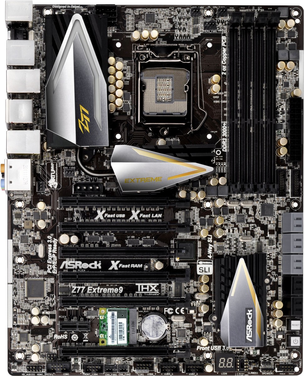
The memory slots feature a single ended design, a style that is starting to become commonplace on mainstream chipsets. Along the right hand side of the board going from top to bottom, we have the standard ATX power connector, followed by two USB 3.0 headers powered by an Etron controller. The position of these USB 3.0 headers indicate the purpose of front ports, as alluded to by the inclusion of a USB 3.0 front panel box. The other header is thus for new cases that support USB 3.0. It should be noted that these headers are four of the X77 Extreme9’s 12 supported USB 3.0 ports.
Underneath the USB 3.0 are the SATA ports – here we have six in grey indicating SATA 6 Gbps (top four are ASMedia, next two are Intel) and four in black for SATA 3 Gbps (Intel). We also find a power button and reset button underneath the SATA ports. The chipset heatsink for the Z77 Extreme9 Is the same size as that found on the Z77 Extreme6, but features ASRock’s white heatsink LED lighting when turned on.
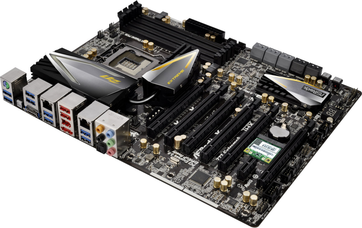
The south side of the board is crammed with headers and functionality for the user. One point should be made however – by using a fourth dual-slot GPU in the bottom slot, most of these headers become almost unusable. My power/reset front panel connectors were sitting such that the fourth GPU was slightly raised, reducing pin-to-pin contact. Nevertheless, we have access to the front panel header, a ClearCMOS jumper, the BIOS itself, a two-digit debug display, three USB 2.0 headers, an IEEE1394 header and a COM header.
The PCIe routing is such that users can either utilize the second PCIe at x16, or use PCIe1/PCIe3/PCIe5/PCIe7 in x16/-/x16/- or x8/x8/x8/x8 (or x8/x8/x16/- and x16/-/x8/x8 for tri-GPU). PCIe4 is only a PCIe 2.0 that runs at x4 (thanks to a PCIe 2.0 PLX chip), and PCIe6 is our aforementioned x1 slot.
Users will also note the molex connector above the PCIe slots. In some motherboards this is there to provide power to the PCIe, or to act as an additional ground to ensure stability. With a full gamut of GPUs, pulling 300W through the 24-pin ATX connector is not a recommended setup, however the ASRock Z77 Extreme9 was able to do it without the 4-pin molex connected. I am not a big fan of having a molex connector for additional power (either a SATA connector or 6-pin PCIe is preferred), and I definitely am not keen on having it directly above the PCIe slots. Having it in this location means that cables from the PSU are going to be stretched over the GPUs or around the board to fit, which negates any nice aesthetics the user is trying to create with a board inside the case. (Note, on the X79 Extreme11, ASRock provide a molex on the bottom of the board at right angles, which is preferred.)
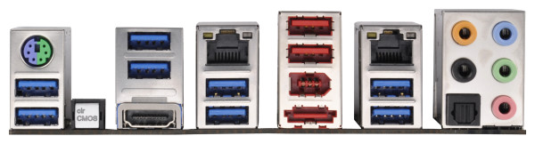
The rear IO forgoes the majority of the Ivy Bridge video connections, leaving only a solitary HDMI port. This allows ASRock to populate the rear IO with a multitude of ports. From left to right, we have a combination PS/2 port, eight USB 3.0 (blue), a clear CMOS button, the HDMI port, dual GbE (Broadcom), two USB 2.0 (red), IEEE1394, eSATA, optical SPDIF output, and audio jacks. In my view, if I was forced to only use HDMI as my video output, I would probably have designed something like this – perhaps removing the left hand side PS/2 + USB 3.0 combination for a single 4-port USB 2.0 interface. Though it is worth mentioning that the HDMI port is limited to 1920x1200 outputs by virtue of the Ivy Bridge iGPU limitation – only DVI-D and DisplayPort will do above this.
Board Features
| ASRock Z77 Extreme9 | |
| Price | Link |
| Size | ATX |
| CPU Interface | LGA-1155 |
| Chipset | Intel Z77 |
| Memory Slots |
Four DIMMs, Supporting up to 32GB DDR3 1066-3000+ MHz, Non-ECC |
| Video Outputs | HDMI |
| Onboard LAN | 2 x Broadcom BCM57781 |
| Onboard Audio | Realtek ALC898 |
| Expansion Slots |
2 x PCIe 3.0 x16 (x8 when GPU used in slot underneath) 2 x PCIe 3.0 x8 1 x PCIe 3.0 x16 (disabled if other slots used) 1 x PCIe 2.0 x1 1 x mPCIe for WiFi+BT Module |
| Onboard SATA/RAID |
2 x SATA 6 Gbps (Intel), Supporting RAID 0, 1, 5, 10 4 x SATA 3 Gbps (Intel), Supporting RAID 0, 1, 5, 10 4 x SATA 6 Gbps (ASMedia ASM1061) SATA3_A4 shared with eSATA3 |
| USB |
4 x USB 3.0 (Intel) [4 back panel] 8 x USB 3.0 (Etron EJ188) [4 back panel, 4 onboard] 8 x USB 2.0 (Intel) [2 back panel, 6 onboard] |
| Onboard |
6 x SATA 6 Gbps 4 x SATA 3 Gbps 1 x mPCIe 1 x COM Header 1 x LED Header 6 x Fan Headers 1 x Molex Power Connector 3 x USB 2.0 headers 2 x USB 3.0 headers Power/Reset Switch ClearCMOS Switch Two-digit Debug |
| Power Connectors |
1 x 24-pin ATX Power Connector 1 x 8-pin CPU Power Connector 1 x Molex Power Connector |
| Fan Headers |
2 x CPU (4-pin, 3-pin) 3 x Chassis (4-pin, 2x 3-pin) 1 x PWR (3-pin) |
| IO Panel |
1 x Combination PS/2 Port 1 x HDMI Port 1 x Optical SPDIF Output 2 x USB 2.0 (red) 8 x USB 3.0 (blue) 1 x eSATA 3 Gbps 2 x Ethernet (Broadcom) 1 x IEEE1394 1 x ClearCMOS Audio Jacks |
| Warranty Period | 3 Years |
| Product Page | Link |
Compared to the other motherboards in this review, the ASRock Z77 Extreme9 comes joint bottom in the list of available video outputs. The ASRock storms ahead in terms of USB 3.0 and SATA ports, and the fact that both the Broadcom NICs can be teamed may be of benefit to some users.
ASRock Z77 Extreme9 BIOS
If my initial outburst in the overview of the ASRock Z77 Extreme9 passed you by, I will quickly go over it again:
When reviewing the Z77 Extreme6, ASRock were slightly disappointed that the board did not match the Gigabyte and ASUS motherboards for performance, due to the their use of MultiCore Enhancement (MCE) for more MHz under full CPU use. ASRock quickly offered me a BIOS with MCE enabled, but this was after I finished the review and not immediately available to the public, so I refused. I informed them when I would be reviewing the Z77 Extreme9, giving them ample time (~4 weeks) to make ready a public BIOS for the board which I would update for testing. When it came around to testing however, the BIOS was not MCE enabled by default.
At the time of testing, the latest BIOS available was 1.50. Since then however, the latest BIOS on the website is now 1.40. Under the changelog for the 1.40 BIOS, it says that it offers a ‘non-K OC’ mode, suggesting that some form of overclocking or MCE is enabled for non-K processors. But MCE for K processors is not present, and thus the Z77 Extreme9 falls behind in terms of performance in benchmarks requiring more than one or two cores.
Nevertheless, the ASRock BIOS is easy to understand. Back at the start of P67, the ASRock P67 Extreme4 was the first motherboard with a graphical interface that I encountered. Since then, the basic layout premise has been maintained, but it certainly looks a lot cleaner. Even more so now given that it has now started to become standard that BIOSes have screenshot buttons, rather than pointing a camera at a monitor:
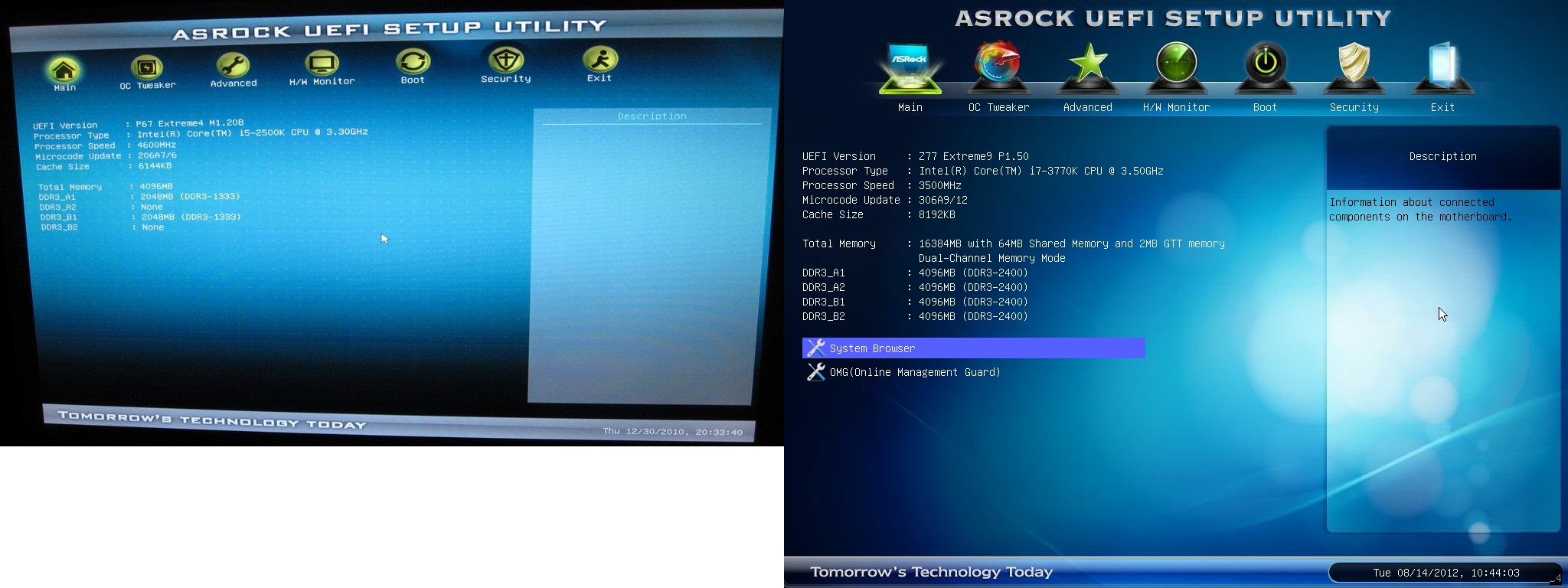
ASRock P67 Extreme4 vs. ASRock Z77 Extreme9
On the front screen, we get a nice amount of information about the system – the motherboard, the BIOS version, the processor (and speed), and the memory (with speeds). What the BIOS is missing is a direct list of temperatures, fan speeds and voltages on this screen though, just as a quick reference for system builders and diagnosis for issues that may arise. There is also scope to present this information in a myriad of ways under the graphical theme.
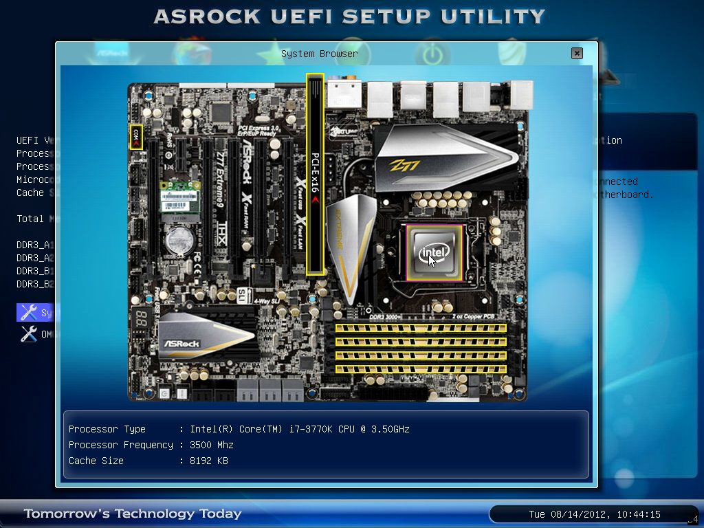
Alongside this data on the main screen, ASRock are putting two features forward which we have observed on the other Z77 motherboards. The first is their system browser, which is essentially a 2D version of Gigabyte’s ‘3D’ BIOS without the extra controls. However, it does allow users to see what is installed on the motherboard and where, and to also identify if it is correctly recognized at POST.
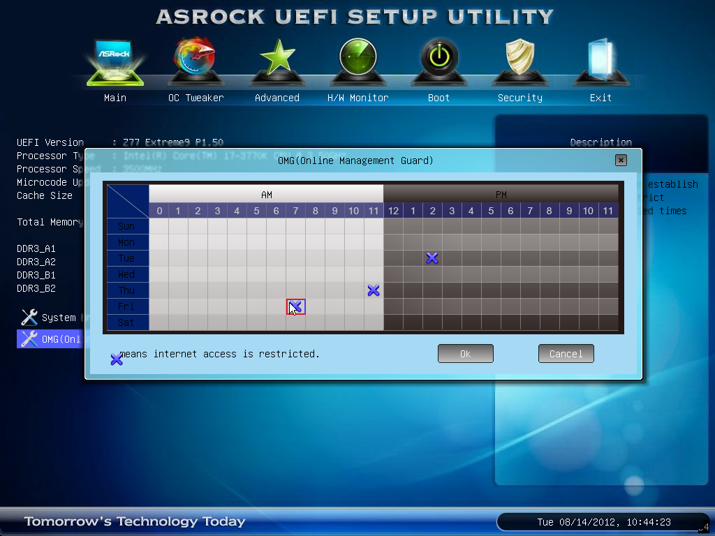
The other feature is the Online Management Guard, or called by the more eye-rolling acronym, OMG. This gives the user control over when the network ports should be enabled or disabled, related to the system time. Should a parent want their child’s internet access stopped by 10pm every night, here is an opportunity to set it. The only way it could be re-enabled is by a user (or child) going into the BIOS and adjusting the settings. The alternative is that the user (or child) could end up using a search engine to find a solution and coming across this review. Once the user (or child) has found away around the problem, the utility of OMG is essentially null and void. Also, it really needs a software interface in the OS, which is currently not provided.
The bulk of the interest of the BIOS will be in the OC Tweaker menu. In this menu, we have a selection of automatic overclock options, from the ‘Advanced Turbo 30’ to the ‘Optimized CPU OC Setting’. The former applies CPU voltage, load line calibration, and a 47x multiplier, whereas the latter offers more conservative settings from 4.0 GHz to 4.8 GHz in 200 MHz increments. These settings are tested in our overclock section for this board.
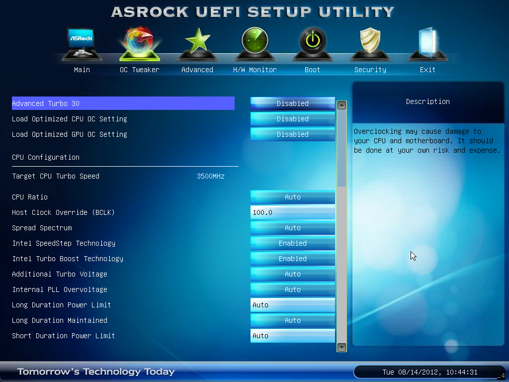
Personally I prefer motherboards where the users can define the CPU multiplier, additional voltage for the turbo mode and power limits all in one menu. To be honest, I had no reason to raise the power limits above automatic for air/water overclock testing. The ASRock also took my XMP profile first time, which in the past on other boards has not always been the case. It is also handy for the voltage and load line calibration settings that ASRock provide an image/explanation of what each setting does, to avoid confusion.
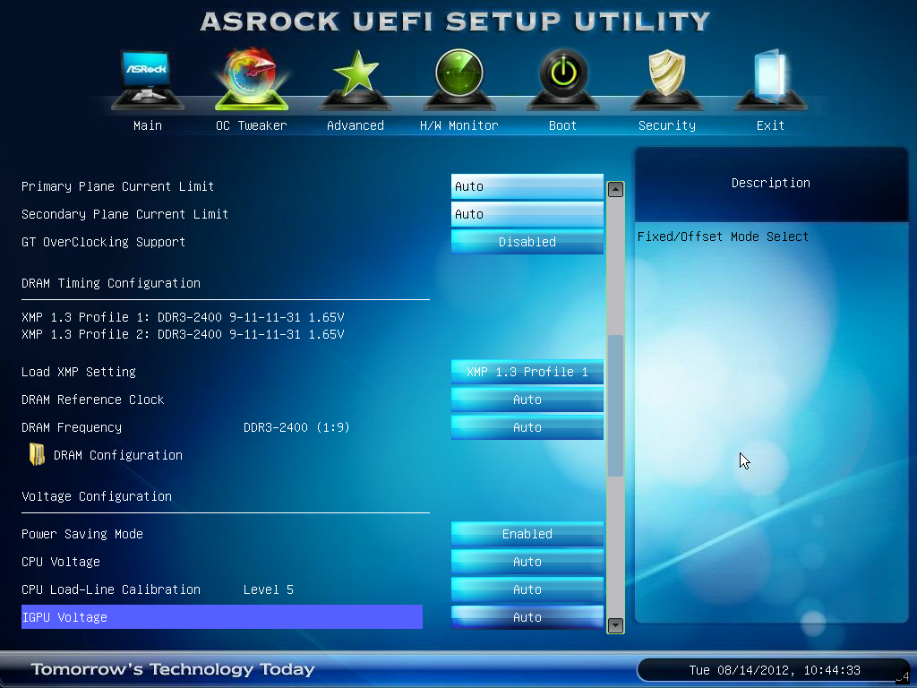
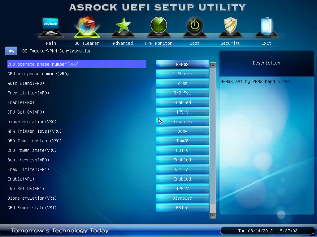
New on the ASRock series is their PWM configuration menu. This is usually attached to digital power solutions, and gives the user control of power limitations and calibrations relating to voltage and OCP. However, for ASRock PWM configuration means something else. Insert a menu of random options that I have no idea what they mean:
An important feature that ASRock have put into their BIOSes is for users to update the BIOS via a direct online connection from within the BIOS. This means that inside the BIOS file is a version of the network driver, and ASRock have programmed this to check the online servers for the latest version. This works great if you are directly connected via Ethernet to a DHCP source, but not for WiFi over USB or for an ICS home network reliant on self-DHCP.
If the internet is unavailable through a network cable, then users can place the latest BIOS on a USB stick and also update it through the GUI.
All the fan controls are located in the H/W Monitor menu, which also showcases temperatures, fan speeds and voltages (note, some of this information should be copied into the Main screen menu). Fan controls have the opportunity to be the simplest functions on the board, however some manufacturers do not put in the effort to make easy-to-understand scales. ASRock meet the user halfway, giving options for target temperatures and fan speed ‘modes’ from Level 1 to 9/10 which adjust the fan ramp up profile as required.
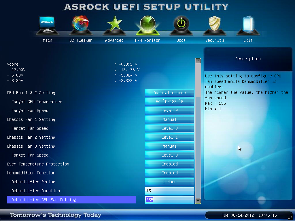
The last feature worthy of note is ASRock’s ‘Dehumidifier’ function. As mentioned in previous reviews, the act of this function is to spool up the fans in climates which vary between very hot during the day and very cold at night. As the temperature rises and falls, if the humidity is in the wrong direction, it could potentially cause condensation in confined areas – for example in the case. The ‘dehumidifier function’ will cause the fans to spin up and equilibrate the temperatures and relative humidity inside and outside the case. What this feature would really benefit from, apart from a name change, is the controls to be available in software as well.


ASRock Z77 Extreme9 Software
Through our Z77 testing, we have come across several ASRock motherboards – the Z77 Extreme4, the Fatal1ty Z77 Professional and the Z77 Extreme6. Aside from the differing color scheme of the Fatal1ty range, the software on the ASRock Z77 series follows a similar format throughout. ASRock are keen to promote their ‘555 XFast’ system, featuring XFast USB, XFast LAN and XFast RAM, which are both advertised to ‘increase speeds by up to 5x’ depending on the specific benchmark in question. We look at these in turn below.
One point of contention is that ASRock is currently the only manufacturer that I have tested that installs Lucid Virtu MVP by default along with the basic driver suite. This can lead to some errors during gaming if users do not realize it is enabled by default.
The main center of ASRock’s software package comes from the ASRock eXtreme Tuning Utility, or AXTU.
ASRock eXtreme Tuning Utility
AXTU features a lot of the controls we would expect in the OS, such as the fan controls, overclocking or power saving utilities. It also provides the user with temperatures, fan speeds and voltages.
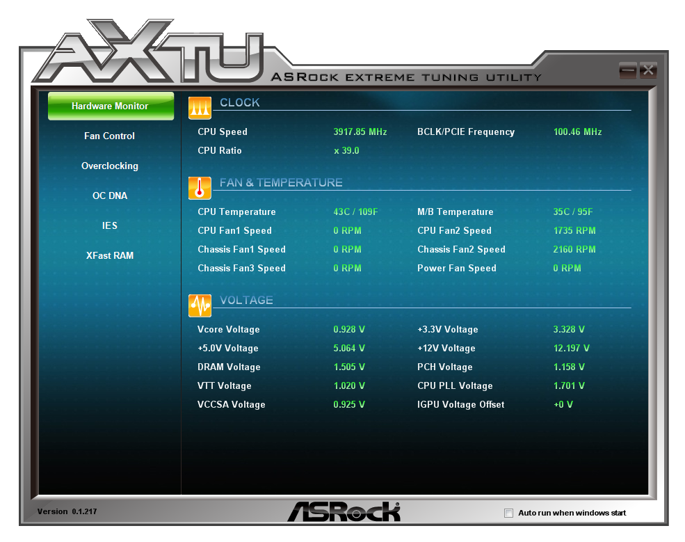
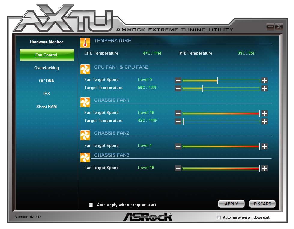
Fan controls in AXTU are similar to those found in the BIOS, with certain fans being given options of a target temperature, and all of them having a ‘target speed’ from Level 1 to 10 which dictates how the fans ramp up. This is by no means any definitive fan control – other manufacturers provide better controls, such as dynamic testing and combination fan/temperature analysis. There is definite scope for improvement from ASRock.
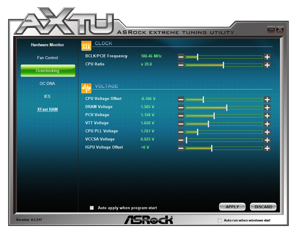
The overclock controls are also a little basic, with only BCLK control directly available without a reboot. The user can manipulate the CPU ratio and voltages, but there is no control over turbo boost ratios, or provided options for levels of overclock testing. In fact, during my testing using the version of AXTU provided on the driver DVD, the program was continuously giving errors if I tried to manipulate any of the voltages.
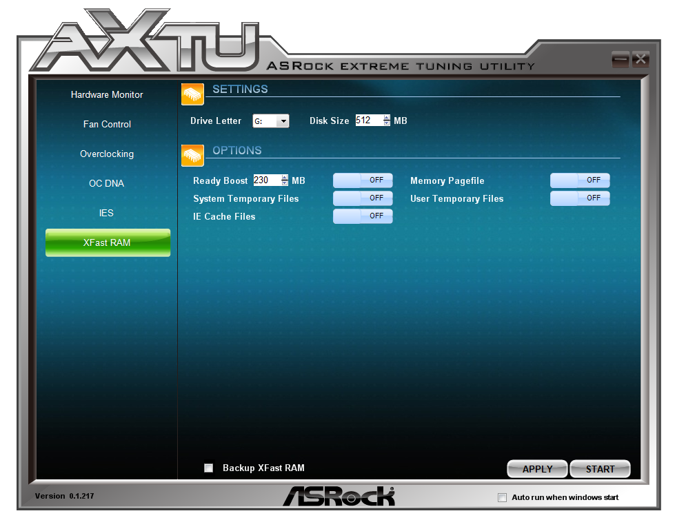
Aside from the ‘Intelligent Energy Saver’ utility that reduces CPU phase usage at the expense of potential longevity, the other main utility in AXTU is XFast RAM. The idea behind XFast RAM is to partition off part of the DRAM onboard for use as a quick cache access for the system page file, for temporary internet files, or perhaps certain programs.
XFast USB
ASRock’s XFast USB is licensed software that ASRock includes with their package, and has done for at least a couple of years now. The premise behind ASRock USB is that the Windows 7 USB driver is flawed, and only accepts basic commands. By injecting a new driver when a device is plugged in, ASRock takes advantage of a new set of commands called BOT (Bulk Only Transfer), which offer faster throughput speeds at the expense of latency. All USB controllers and devices support BOT - the step up from BOT is called UASP, which is what ASUS implement via a hardware (ASMedia controller) and software implementation. In Windows 8, the OS should be able to use the best of BOT or UASP, depending what the controller onboard supports.
The downside to XFast USB over ASUS’ solution is that XFast is limited to one USB device at a time, and plugging in a device for the first time requires a user to remove and reinsert it to get the XFast speedup. XFast beats UASP for sequential transfers, but UASP offers many magnitudes of improvement for small file transfers, making UASP preferential for regular USB read/write activity rather than storage.
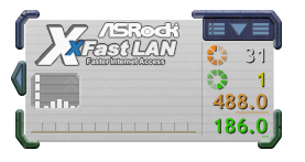
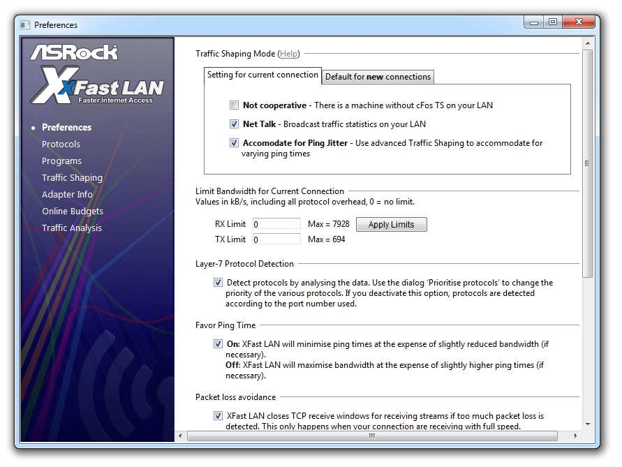
XFast LAN
Another licensed bit of software for ASRock is XFast LAN, which is an ASRock branded version of cFosSpeed, available for around 10-15 euros. This software allows users to prioritize programs for network use, as well as monitor throughput:


ASRock Z77 Extreme9 In The Box
ASRock boxes can often flip between very good value and perhaps not so much. On the plus side, they had a phase where even the cheap end boxes contained a USB 3.0 front panel addition, which I thought was quite special. In terms of the Z77 Extreme9, we get the following:
Driver CD
IO Panel
Manual
Six SATA cables
Two SATA-to-Molex Power Cables
3-way Rigid SLI Bridge
Three 2-way SLI Bridges
Wi-SB Box
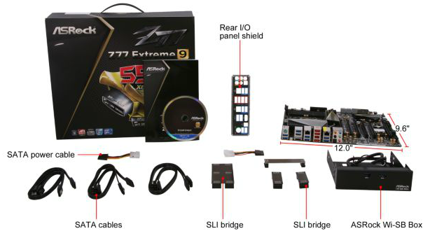
While the ASRock Z77 Extreme9 has more SATA ports than the Gigabyte G1.Sniper 3, they have decided to put less SATA cables in the box – we do not get anything eSATA or otherwise either. The big plus in the box is the ASRock Wi-SB box, which connects to the onboard WiFi. This Wi-SB box houses two sets of antenna, allowing for better reception of WiFi signals. The box doubles up as a 2.5” drive storage and two USB 3.0 ports for use on one of the two USB 3.0 headers.
Voltage Readings
After my first publication of OCCT voltage readings, a few readers responded with a more in-depth reasoning behind some of the results we were seeing. With this in mind, I would like to re-describe what we are doing with this test, and how it comes about.
Much of what an enthusiast overclocker does is monitor CPU temperature and voltage. Whatever settings a user places in the BIOS or OS is at the mercy of the motherboard - in terms of actually setting the values and reporting the values back. As an enthusiast, we have to rely on what readings we get back, and hope that motherboard manufacturers are being honest with their readings.
Take CPU voltage. What we as a user see in CPU-Z or OCCT is a time-averaged value that hides voltage ripple (if any) for power delivery. It is very easy for a motherboard manufacturer to hide this value, or to disregard slight deviations and report a constant value to the user. The CPU voltage reading can be taken at a variety of places on the power plane, which can vary between motherboards and manufacturers, meaning that each reading is essentially not comparable with the other. Nevertheless, as an enthusiast, we will constantly compare value A with value B.
Whether or not I can achieve 4.7 GHz with 1.175 volts on a particular board is inconsequential - your motherboard may perhaps produce the same result with a reading at 1.200 volts. The only way to test the actual value is with consistent methodology is via an oscilloscope connected to similar points on each board. This may sound like taking an OCCT reading is therefore redundant.
However, motherboards have settings relating to load line calibration. As load is applied to the CPU, the voltage across the processor decreases (VDroop). Load Line calibration essentially attempts to control this level of droop, by increasing voltage when voltage drops are detected away from a fixed value. Manufacturers have different ideas on how to modify LLC with respect to load, or whether the level of modification should be controlled by the user. Some manufacturers offer the option at a variety of levels, such that overclockers can be sure of the applied setting (even if it increases peak voltage, as explained by AnandTech in 2007).
By doing a full load OCCT test, we are essentially determining both how aggressive the motherboard is reporting the CPU voltage under load and how aggressive load line calibration is performing (from the point of view of the user without an oscilloscope or DVM). If someone has one of the motherboards we have tested and you have a different one, variations in load voltage should describe the offset you may require for overclock comparisons.

As seen on other ASRock motherboards, the CPU at load in an ASRock board tends to be a little jumpy in terms of what is reported to the operating system. The reports have a 0.008 volt granularity, which could mask a much smaller variation over time. Though our OCCT recording is actually a smoothing over time, so for the OCCT reading to jitter so much does lead to a mild concern. I also ran the test in an overclocked setting, with LLC set at Level 1:
There was still mild jitter being recorded on a heavily overclocked system, which leads me to believe that this is something systemic while the system is at load.
| Reported Load Voltage / V | |
| ASRock Fatal1ty Z77 Professional | 0.956 |
| ASRock Z77 Extreme4 | 1.050-1.058 |
| ASRock Z77 Extreme6 | 1.040-1.048 |
| ASRock Z77 Extreme9 | 1.016-1.024 |
| ASUS P8Z77-V Deluxe | 1.085 |
| ASUS P8Z77-V Pro | 1.090 |
| ASUS P8Z77-V Premium | 1.088 |
| Biostar TZ77XE4 | 1.036 |
| ECS Z77H2-AX | 1.048 |
| EVGA Z77 FTW | 0.698-0.706 |
| Gigabyte Z77X-UD5H | 1.067 |
| Gigabyte Z77X-UD3H | 1.067 |
| Gigabyte G1.Sniper 3 | 1.068-1.078 |
| MSI Z77A-GD65 | 1.020 |
ASRock Z77 Extreme9 Overclocking
Note: Ivy Bridge does not overclock like Sandy Bridge. For a detailed report on the effect of voltage on Ivy Bridge (and thus temperatures and power draw), please read Undervolting and Overclocking on Ivy Bridge.
Experience with ASRock Z77 Extreme9
Overclocking with the ASRock Z77 series of motherboards is actually quite easy compared to some of the others. ASRock offer a good selection of automatic overclocking controls, from the ‘Advanced Turbo 30’ to the ‘Optimized CPU OC Setting’ options, and for manual selections we have direct access to CPU multipliers, BCLKs, voltages and LLC all in a single screen. Failed CPU overclocks are easily caught, but the downside to the ASRock OC functionality is their operating system software, which does not amount to much.
*It should be noted that during the overclock testing of this motherboard, the localized temperature was higher than usual due to the weather. We experienced similar issues with the ASUS P8Z77-V Premium, and as a result our overclock limits were hit earlier than expected. As explained in the ASUS review, it is hard to keep temperatures constant under these circumstances in the UK where air conditioning is not a standard feature in properties. In this case, I added a pair of fans to aid in cooling.
Methodology:
Our standard overclocking methodology is as follows. We select the automatic overclock options and test for stability with PovRay and OCCT to simulate high-end workloads. These stability tests aim to catch any immediate causes for memory or CPU errors.
For manual overclocks, based on the information gathered from previous testing, starts off at a nominal voltage and CPU multiplier, and the multiplier is increased until the stability tests are failed. The CPU voltage is increased gradually until the stability tests are passed, and the process repeated until the motherboard reduces the multiplier automatically (due to safety protocol) or the CPU temperature reaches a stupidly high level (100ºC+).
Our test bed is not in a case, which should push overclocks higher with fresher (cooler) air. We also are using Intel's All-in-one Liquid Cooler with its stock fan. This is a 120mm radiator liquid cooler, designed to mimic a medium-to-high end air cooler.
Automatic Overclock:
The automatic overclock options are in the BIOS, found directly at the top of the OC Tweaker menu. The main two options are ‘Advanced Turbo 30’, which implements a 4.7 GHz overclock with aggressive voltage timings, or ‘Optimized CPU OC Setting’, which applies presets from 4.0 GHz to 4.8 GHz with a less aggressive strategy.
Here are our results:
For the Advanced Turbo 30 setting, the system applied an all-core overclock to the 47x multiplier along with a +0.085 volt offset on the CPU under LLC Level 1. The system also applied a +0.120 volt offset to the iGPU, along with iGPU LLC Level 2. At these settings, the system showed 1.280 volts at load in the OS, with peak temperatures during PovRay reaching 102°C and during OCCT of 103°C. In both cases, the system declocked down to 46x to reduce temperatures.
With the ‘Advanced CPU OC Settings’, we have options from 4.0 GHz to 4.8 GHz in 200 MHz intervals. The following results were obtained.
At the 4.0 GHz setting, the system remained at automatic CPU voltages and LLC settings. In the OS, a load voltage of 1.168 volts was reported, and peak temperatures observed were 79°C for PovRay and 84°C for OCCT.
At the 4.2 GHz setting, the system remained at automatic CPU voltages and LLC settings. In the OS, a load voltage of 1.176 volts was reported, and peak temperatures observed were 83°C for PovRay and 87°C for OCCT.
At the 4.4 GHz setting, the system remained at automatic CPU voltages and LLC settings. In the OS, a load voltage of 1.176 volts was reported, and peak temperatures observed were 86°C for PovRay and 87°C for OCCT.
At the 4.6 GHz setting, the system remained at automatic CPU voltages but adjusted the LLC to Level 1. In the OS, a load voltage of 1.192 volts was reported, and peak temperatures observed were 87°C for PovRay and 91°C for OCCT.
At the 4.8 GHz setting, the system gave a fixed CPU voltage of 1.240 volts and adjusted the LLC to Level 1. In the OS, a load voltage of 1.224 volts was reported, but the system was unstable, giving errors in both PovRay and OCCT.
Manual Overclock:
In the manual overclocking, the system was adjusted to LLC Level 1 from the beginning, to allow for greater stability at high CPU loading. As usual for Z77 overclocks, we start at the 44x multiplier and 1.100 volts in the BIOS with our i7-3770K CPU.
At the 44x multiplier, the system was stable at a minimum BIOS voltage of 1.100 volts. This showed a load voltage of 1.096 volts in the OS, and peak temperatures of 76°C during PovRay and 78°C during OCCT.
At the 45x multiplier, the system was stable at a minimum BIOS voltage of 1.100 volts. This showed a load voltage of 1.104 volts in the OS, and peak temperatures of 77°C during PovRay and 79°C during OCCT.
At the 46x multiplier, the system was stable at a minimum BIOS voltage of 1.150 volts. This showed a load voltage of 1.152 volts in the OS, and peak temperatures of 84°C during PovRay and 87°C during OCCT.
At the 47x multiplier, the system was stable at a minimum BIOS voltage of 1.200 volts. This showed a load voltage of 1.208 volts in the OS, and peak temperatures of 92°C during PovRay and 94°C during OCCT.
At the 48x multiplier, the system was not stable even at 1.275 volts in the OS. At this voltage, the system would rise to above 100°C in PovRay and give memory errors.
ECS is a much larger company than most consumers realize. Selling to end users is not its primary market – over three quarters of all their sales are to OEMs in Pan-Asia. Over the past couple of years, we have had two group interviews with their Vice President of Channel Business, David Chien (2011, 2012), and the consensus has been to push into the retail market. This has been met with varying degrees of success, from tales of woe to indifference or being pleasantly surprised (such as with their X79R-AX, a very cost efficient X79 motherboard). As part of this review we were shipped the ECS Z77H2-AX, a product designed to appeal to users aesthetically and as part of the ‘Golden’ range ECS wants to market.
ECS Z77H2-AX Overview
Truth be told, the first few minutes of testing a motherboard often dictates how the whole testing feels. My first task is usually to update the BIOS, via USB stick, followed by setting XMP and installing the operating system on AHCI mode. Unfortunately, the ECS Z77H2-AX falls down on all three accounts. I was unable to update the BIOS through the BIOS itself and as such had to install the operating system; XMP with my regular memory set did not work at all (we settled for something close); and by default the BIOS puts SATA modes in IDE, even on the latest BIOS.
The big draw over the ECS Z77H2-AX is meant to be the ‘Golden Board’ motif, and the fact that the majority of the board is swathed in a metallic gold paint. ECS wants modders to abuse this fact with the golden ECS GTX 680 that is on the market, and produce a thing of beauty. When I unboxed this motherboard I happened to have some family around, and they commented heavily on the styling having been dazed by the gold color.
Along with the memory not being at XMP (we settled for DDR3-2133 10-12-12), the ECS Z77H2-AX does not have MultiCore Enhancement for that extra MHz boost during heavy workloads. As a result, the ECS does not hit the heights of ASUS and Gigabyte in this regard. We also found a distinct issue with the USB 2.0 routing, whereby even straight forward sequential testing from the IO panel was bottlenecked down from 32-34 MBps that we normally see to 25 MBps.
When I test, I write notes down of all the features and foibles that a motherboard has. Out of this combination review, the ECS Z77H2-AX wins the prize for the most observable issues. For example, this roundup is focusing on motherboards that contain the PLX PEX 8747 chip – the ECS is different to all the other manufacturers in the sense that it only offers three full PCIe slots from the PLX chip, in a 16x/8x/8x layout. This is a good idea – there are very few users who need a full set of four-way PCIe lanes. However, during my testing, I discovered that the third slot cannot be used for GPUs. With three HD 7970s connected, I had no output through any of the GPUs, even though the system seemed to enter the operating system without fuss. Another kicker was in dual GPU mode – on every other product I have tested, the video is output from the top card. Not so with the ECS Z77H2-AX, whereby the video comes out the second card – strange indeed.
In terms of features, we get WiFi and Bluetooth on the IO panel, and an mSATA port on board. Unlike other boards in this review, we do not get dual NIC, we have only six total USB 3.0 ports, only one extra SATA controller, Realtek ALC892, and only three fan headers. We also end up with a BIOS that is harsh on colorblind users (I had issues, and I am partially red/green colorblind), and a software package that needs a revamp. All of this for $310 is a hard sell, especially when other products have a better all around package. In this case, the money is going on the looks rather than the substance, unfortunately.
Visual Inspection
If all you ever wanted in live was something colored gold, I think ECS have you covered. As part of their Golden Board branding, the ECS Z77H2-AX has figuratively been gold plated. The heatsinks, heatpipes, socket, capacitors, VRMs and IO panel have all had a layer of gold paint added in order to improve aesthetics. When I first took this board out of the wrapper, I was figuratively blinded by just how much of the gold color was in my face.
The socket area is surrounded on three sides by large golden colored heatsinks, and the other side by the memory slots, giving the minimum Intel specified distance for coolers. The power delivery heatsinks rise approximately 32mm from the surface of the PCB, suggesting that ECS prefer users with all-in-one liquid coolers to use the Z77H2-AX. This is despite the lack of fan headers around the board – we have one 4-pin header for the CPU to the top-right of the socket, and a 3-pin the other side of the memory. The final fan header (4-pin) is on the south side of the board. It should be noted that the heatsinks are connected via heatpipes into pairs – the ones covering the power delivery as one pair, and the heatsink covering the PLX 8747 chip underneath the socket is connected to the chipset heatsink.

It is also worth mentioning the location of the 8-pin CPU power connector, which is a lot further into the motherboard than on most models, potentially causing issues for bottom mounted power supply setups and cable management.
Along the right hand side of the motherboard from top to bottom we get one of the fan headers (3-pin), the 24-pin ATX power connector, a pair of power/reset buttons, and the SATA ports. The layout of the SATA ports on this motherboard is a little odd – we get access to four SATA 6 Gbps internal ports, two from the Z77 chipset and two from an ASMedia controller, but ECS have decided to use only three of the four SATA 3 Gbps from the chipset. Two of these are the differently shaped SATA ports at the bottom, one is used by the mSATA port, and the fourth is not present on the board at all. My first thought was perhaps they are related to the eSATA ports on the IO back panel, but these are powered by their own controller. Typically other manufacturers add the extra ports, and you get a choice between the mSATA or one of the SATA 3 Gbps ports – ECS does not offer that choice. I would have thought that at least a SATA header coming out of the board would have been thought of. Also on the right side of the board we have a two-digit debug display, that judging by the printing on the PCB should double up as a temperature sensor readout in the operating system – default functionality just gave me an ‘A0’ reading, suggesting this feature is not working.
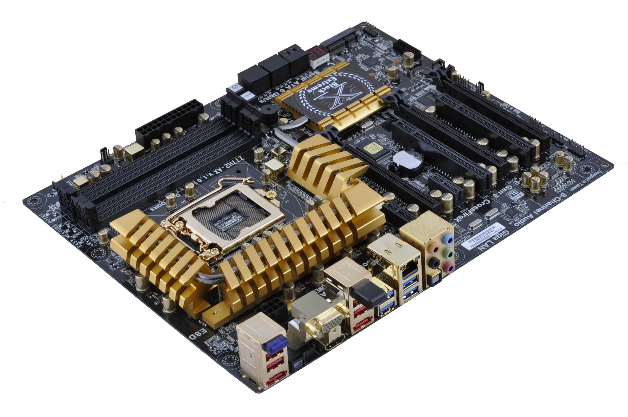
Along the bottom of the board, ECS are also a little sparse on the header arrangement. The Z77 chipset allows for twelve USB 2.0 ports through a combination of back panel connectors – here we get access to only six in total. The USB 2.0 header onboard supports ECS’ EZ Charger technology, whereas another oddity on board is that ECS use a Texas Instruments branded USB 3.0 controller for their onboard header. This is the first time we have encountered a TI branded USB 3.0 header, which suggests that there is a deal between the companies and ECS find it cost effective. Unfortunately, the BOM cost for each of the different controllers is not directly available to us, and each company is likely to have a unit deal in the works.
The PCIe layout is one of the marketable design elements on the motherboard. ECS has gone for three full-length PCIe slots powered from the PLX chip, which means the slots are organized such that there is a three slot gap between the first and the second. We get access to a short x1 slot at the top (blocked by the large PLX heatsink), and due to onboard controllers, access to two PCI slots for legacy devices.

The IO panel, while swathed in a gold color, is actually well thought out. From left to right, we get a Bluetooth module, four USB 2.0 ports (red), two eSATA 6Gbps ports, a ClearCMOS button, a VGA output, a HDMI output, a WiFi module (black), four USB 3.0 ports (blue), gigabit Ethernet (Realtek), audio jacks and a SPDIF output. Actually, one point should be made: from the Ivy Bridge processors, only two connections allow a greater than 1920x1200 output – DVI-D and DisplayPort. None of them are here, meaning that for IGP setups, 1920x1200 is your limit.
Board Features
| ECS Z77H2-AX | |
| Price | Link |
| Size | ATX |
| CPU Interface | LGA-1155 |
| Chipset | Intel Z77 |
| Memory Slots |
Four DIMMs, Supporting up to 32GB DDR3 1066-2133+ MHz, Non-ECC |
| Video Outputs |
VGA HDMI |
| Onboard LAN | Realtek 8111E |
| Onboard Audio | Realtek ALC892 |
| Expansion Slots |
1 x PCIe 3.0 x16 1 x PCIe 3.0 x16 (x8 when GPU in first slot) 1 x PCIe 3.0 x8 2 x PCIe 2.0 x1 2 x PCI |
| Onboard SATA/RAID |
2 x SATA 6 Gbps (Intel), Supports RAID 0, 1, 5, 10 2 x SATA 3 Gbps (Intel), Supports RAID 0, 1, 5, 10 2 x SATA 6 Gbps (ASMedia), Supports RAID 0, 1 1 x mSATA 3 Gbps |
| USB |
4 x USB 3.0 (Intel) [4 back panel] 2 x USB 3.0 (TI TUSB7320) [2 onboard] 6 x USB 2.0 (Intel) [4 back panel, 2 onboard] |
| Onboard |
4 x SATA 6 Gbps 2 x SATA 3 Gbps 1 x mSATA 3 Gbps 1 x USB 3.0 Headers 1 x USB 2.0 Header 3 x Fan Headers 1 x COM Header Power/Reset Buttons Debug LED |
| Power Connectors |
1 x 24-pin ATX Power Connector 1 x 8-pin CPU Power Connector 1 x 4-pin Molex Power Connector |
| Fan Headers |
1 x CPU (4-pin) 1 x SYS (3-pin) 1 x PWR (3-pin) |
| IO Panel |
4 x USB 3.0 Ports 4 x USB 2.0 Ports 1 x D-Sub 1 x HDMI 1 x Realtek GbE 1 x ClearCMOS button 1 x WiFi Module 1 x Bluetooth Module 2 x eSATA 6 Gbps Audio Jacks Optical SPDIF Output |
| Warranty Period | 3 Years |
| Product Page | Link |
The main criticism of the ECS Z77H2-AX is its sheer lack of anything exciting. For a motherboard that costs $310 we want something more out of the norm than just a gold color and a PLX PEX 8747 chip. While we do get onboard WiFi and an mSATA port, we are limited to a single NIC, no output capable of more than 1920x1200, only six USB 2.0 ports, an unknown factor in the Texas Instruments USB 3.0 controller, a total of three fan headers and only six normal SATA ports on board. ECS really need to take a good hard look at their BOM for this board, as $310 is cutting the wallet a little deep if you do not care for aesthetics.
ECS Z77H2-AX BIOS
Despite not being a top-tier consumer motherboard vendor, ECS have perhaps put a surprising amount of time into their BIOS GUI representation over the past 18 months. Back in July 2011, we got a sneak peek at the second version of the BIOS GUI, which was officially implemented on the X79 range. This design comes into the Z77 series, with a minor update in terms of an ‘easy-to-use’ front screen.
Unfortunately though, all is not well with the ECS BIOS. The first thing that stood out from my perspective was the easy-to-use screen, which uses a highlighting system to let users know which button is selected. However, as a red/green colorblind user, I can only tell which button is selected if I move the cursor. Perhaps I am being a little harsh as this would only affect a small minority of people, but it would only take someone internally a second or so to tell the BIOS designer to choose contrasting colors.
One main flaw with the ECS BIOS is the ability to recover from default settings. When I first put this motherboard on the test bed, it was a nightmare to work out how to stop the motherboard from restarting with the phrase ‘original settings loaded’. The solution was to load up the BIOS after a ClearCMOS and then manually select ‘default’, then ‘save and exit’. Any more changes that needed to be put in, such as changing the SATA protocol to AHCI from the default IDE (another point of contention), had to be done on a successive reboot. No other motherboard has this ‘flaw’, nor does any previous ECS motherboard, so it is a wonder that we find it here. I noted this several weeks ago, giving ECS time to fix it before I came to a full testing session. As of several days ago, ECS had not updated the BIOS online.
Users should also note that S3 resume is a little odd on this board. Typically during S3 I can wake the system by clicking the mouse or touching the keyboard. No such luck here – the default setting requires the power button to be pressed to wake the system.
As for the BIOS layout, the initial quick BIOS screen looks like this:

The screen offers no quick ‘Save and Exit’ solution unless you select ‘Default’ or ‘Boot’. Normally the F10 button in a BIOS brings up the ‘Save and Exit’ screen, however in the ECS Z77H2-AX, this button is actually F4, and it does not work in this quick mode. The one thing we do get in the first screen though is the CPU model and memory count, although we do not get the motherboard model, current CPU speed, temperatures, voltages or fan speeds. When this screen was being designed by ECS, it would have been fruitful if one engineer or designer had taken a long hard look at some of the options offered by the top tier vendors.
To get inside the main meat of the BIOS, users will navigate through the ‘Advanced’ option. From this we get to the normal looking ECS BIOS GUI:

Similarly here, we get no significant motherboard information.
Users with SSDs will want to jump straight to Advanced -> SATA Configuration to enable AHCI. On all modern motherboards, AHCI is enabled by default, and yet ECS have IDE mode as default. I would like to reiterate my statement regarding having a long hard look at top tier vendor products in this regard.
Due to the limited number of fan headers on board the motherboard, the fan controls are similarly light in their application. Fan controls are found in a sub menu of the PC Health screen under Advanced, and we can only control the CPU fan via its smart mode. Like many of the lower tier manufacturers, rather than actually giving the user a normal scale in terms of RPM % and temperatures, ECS give us arbitrary PWM units in order to set a hysteresis loop. That is one plus point in the ECS book – they are the only manufacturer which allows users to set a temperature/fan control hysteresis. No doubt ASUS would take note with their top-of-the-line fan control system.

Overclocking options are all located in the M.I.B X menu, which compared to some manufacturers layouts is actually easy to follow. On the main screen we get a Quick OC list of settings which in reality means ‘adjust voltages here’. To change between setting a CPU voltage that is fixed versus an offset, the ‘CPU Voltage Mode’ should be changed. One point worth noting is how the board responds in enabling/disabling VDroop, which we detail in the overclocking section.
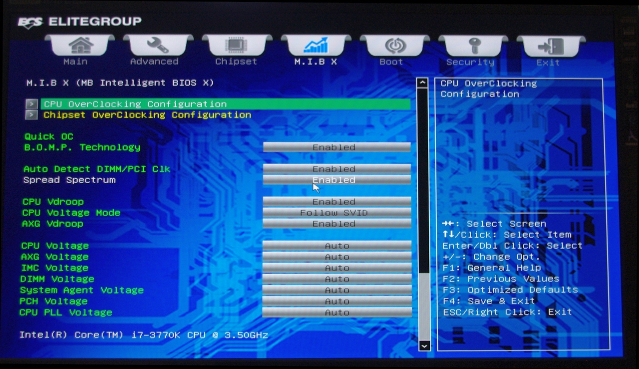
CPU overclock settings are behind the aptly named CPU Overclocking Configuration, though memory overclock settings are listed under the Chipset Overclocking Configuration.


In the CPU menu, the BCLK and Multiplier are easily adjustable within their limits – the user need not worry regarding power limitations. One minor point to note is that the granularity of the BCLK adjustment is only to the 1 MHZ, rather than to 0.1 MHz like on other motherboards.
The memory options give either full automatic settings, XMP settings, or a full manual setting. This is a little frustrating, as it requires the user to know every single minor setting of their memory, many of which are not available to the user unless they are in the operating system with the appropriate software. Other manufacturers offer ‘automatic’ sub-timing settings which ECS do not. I also found that when switching from XMP to manual, the system kept the XMP settings in manual, which helped a little when setting higher memory profiles.
Finally, I must make mention one flaw with the ECS methodology. The system offers only one main way of updating the BIOS – through the operating system using ECS software. Almost every other motherboard manufacturer offers a utility to update the BIOS through a BIOS option or by pressing a particular button at boot. This is frustrating as a reviewer, as I then have to reinstall the OS with the BIOS updated to keep things fair between reviews.


ECS Z77H2-AX Software
Bundled software gives motherboard manufacturers innovative ways of increasing the usability of their products by either in-house design or licensed software. As users, we would ideally like software that is quick to load, takes as few system resources as possible, and every tweakable selection under one executable file. So far, only one manufacturer offers anything close to this, which is a shame when the scope for software potentially outweighs the scope for motherboard design. ECS falls into the other category – with one element of their software package still having the same spelling error since P67.
To start with, the Driver CD offers a silent install for all the main chipset drivers (which is good), except the installation of the Realtek audio driver requires manual interaction (which is undesired). The utilities for use on the motherboard require individual installation, and the main utilities we installed were eSF, eOC, eDLU, and eBLU.
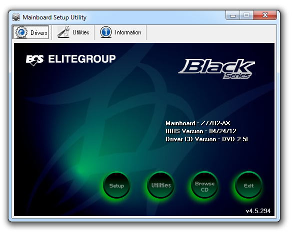
eOC
The main software for ECS motherboards is in the eOC (OC for overclocking), which offers a small monitoring tool for the CPU temperature, the limit to which the system will shut down if the temperature reaches that limit, and some mild overclock settings.
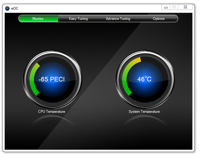
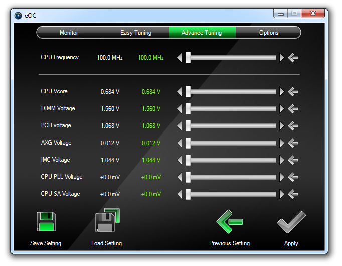
The voltage setting menu is a little odd as it displays the CPU voltage as what the idle voltage is, rather than anything set in the BIOS.
eSF
For the single controllable fan header on the Z77H2-AX, we get software to control it. eSF (SF for Smart Fan) allows users to set a hysteresis curve for the fan header based on fan speed and system temperature. As shown below, three elements of the hysteresis can be set.
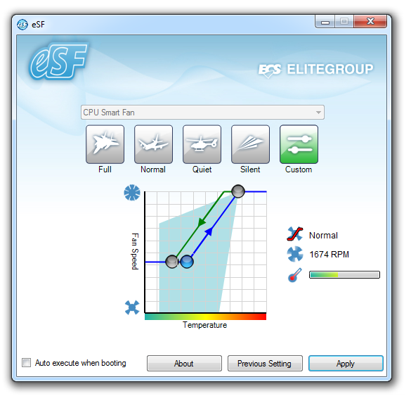
eBLU
eBLU is the BIOS update utility, which will search online for the latest BIOS for the motherboard from ECS’ servers. The system will also update the BIOS from a file.
eDLU
eDLU is the ‘Download Live Update’ utility from ECS, which has been part of the repertoire on ECS motherboards for a good couple of years. The premise is simple – get a list of the latest software and driver versions online from ECS servers and update as required. MSI do this quite well with their software stack, but with ECS things were not as rosy. On clicking the link, my system opened up the browser and showed me a blank page. Absolutely nothing. I tried the next day, and nothing again. It does seem very odd to include a bit of software if the web end does not work for a product that has been out for a couple of months.


ECS Z77H2-AX In The Box
ECS bundles are often an unknown factor, given that ECS boards are not as frequent on our review schedule as some of the others. Given our previous discussion regarding the price and the feature set, we hope that ECS can recoup some of the wow factor by providing a good deal.
Driver DVD
User Manual
Rear IO Shield
Six SATA Cables
Front USB 3.0 panel with rear bracket
SLI Fingers
Protective Caps for unused ports
WiFi Aerial
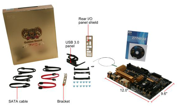
A surprising mix in the box – we are glad to see a full compliment of SATA cables for a Z77 motherboard above $300, as well as a USB 3.0 panel. The protective caps included in the box are odd, as some other manufacturers also provide these but they come attached to the motherboard when shipped, rather than in a plastic bag in the box. The WiFi aerial is also confusing, as it technically has nothing to connect to, like the antenna we get with Gigabyte motherboards or magnetic antenna with ASUS motherboards.
Voltage Readings
After my first publication of OCCT voltage readings, a few readers responded with a more in-depth reasoning behind some of the results we were seeing. With this in mind, I would like to re-describe what we are doing with this test, and how it comes about.
Much of what an enthusiast overclocker does is monitor CPU temperature and voltage. Whatever settings a user places in the BIOS or OS is at the mercy of the motherboard - in terms of actually setting the values and reporting the values back. As an enthusiast, we have to rely on what readings we get back, and hope that motherboard manufacturers are being honest with their readings.
Take CPU voltage. What we as a user see in CPU-Z or OCCT is a time-averaged value that hides voltage ripple (if any) for power delivery. It is very easy for a motherboard manufacturer to hide this value, or to disregard slight deviations and report a constant value to the user. The CPU voltage reading can be taken at a variety of places on the power plane, which can vary between motherboards and manufacturers, meaning that each reading is essentially not comparable with the other. Nevertheless, as an enthusiast, we will constantly compare value A with value B.
Whether or not I can achieve 4.7 GHz with 1.175 volts on a particular board is inconsequential - your motherboard may perhaps produce the same result with a reading at 1.200 volts. The only way to test the actual value is with consistent methodology is via an oscilloscope connected to similar points on each board. This may sound like taking an OCCT reading is therefore redundant.
However, motherboards have settings relating to load line calibration. As load is applied to the CPU, the voltage across the processor decreases (VDroop). Load Line calibration essentially attempts to control this level of droop, by increasing voltage when voltage drops are detected away from a fixed value. Manufacturers have different ideas on how to modify LLC with respect to load, or whether the level of modification should be controlled by the user. Some manufacturers offer the option at a variety of levels, such that overclockers can be sure of the applied setting (even if it increases peak voltage, as explained by AnandTech in 2007).
By doing a full load OCCT test, we are essentially determining both how aggressive the motherboard is reporting the CPU voltage under load and how aggressive load line calibration is performing (from the point of view of the user without an oscilloscope or DVM). If someone has one of the motherboards we have tested and you have a different one, variations in load voltage should describe the offset you may require for overclock comparisons.

While nothing is relatively surprising with the OCCT reading for the ECS Z77H2-AX at stock while under load, I did notice a strange relationship between the voltage set in the BIOS and the voltage reported under load. In the BIOS, if the option for VDroop is disabled, the motherboard should adjust the applied voltage to the processor under load to keep it as constant as possible to that set in the BIOS. So if I set 1.200 volts in the BIOS, VDroop/Load Line Calibration should maintain that 1.200 volts at load. This is not the case. Here are a few set and observed voltages for this motherboard, with VDroop disabled:
- Voltage in BIOS: 1.100 volts
- Voltage in OS at load: 1.164 volts
- Voltage in BIOS: 1.125 volts
- Voltage in OS at load: 1.200 volts
- Voltage in BIOS: 1.200 volts
- Voltage in OS at load: 1.272 volts
The positive bias in the voltage readings is un-nerving. If a user or system builder is used to placing a voltage and overclock on any other Z77 motherboard and attempts the same here, the system will actually apply another 0.064 to 0.075 volts. This will lead to vastly increased temperatures, and perhaps cause overheating. This should not be the case, and I feel that there is perhaps a distinct BIOS programming error here.
| Reported Load Voltage / V | |
| ASRock Fatal1ty Z77 Professional | 0.956 |
| ASRock Z77 Extreme4 | 1.050-1.058 |
| ASRock Z77 Extreme6 | 1.040-1.048 |
| ASRock Z77 Extreme9 | 1.016-1.024 |
| ASUS P8Z77-V Deluxe | 1.085 |
| ASUS P8Z77-V Pro | 1.090 |
| ASUS P8Z77-V Premium | 1.088 |
| Biostar TZ77XE4 | 1.036 |
| ECS Z77H2-AX | 1.048 |
| EVGA Z77 FTW | 0.698-0.706 |
| Gigabyte Z77X-UD5H | 1.067 |
| Gigabyte Z77X-UD3H | 1.067 |
| Gigabyte G1.Sniper 3 | 1.068-1.078 |
| MSI Z77A-GD65 | 1.020 |
ECS Z77H2-AX Overclocking
Note: Ivy Bridge does not overclock like Sandy Bridge. For a detailed report on the effect of voltage on Ivy Bridge (and thus temperatures and power draw), please read Undervolting and Overclocking on Ivy Bridge.
Experience with ECS Z77H2-AX
Previous overclocking attempts on ECS motherboards have not entirely been successful – the name ECS does not exactly scream with an overclocking heritage. If your company background is based in OEM and B2B sales, overclocking expertise is probably not at the front of the mind when a motherboard is made. Despite this, ECS recently paired up with overclocking league website HWBOT as a sponsor and has run competitions for users using ECS motherboards as well as users to win ECS motherboards. Results in these competitions were a little mixed, with the winners having to modify the motherboards physically to reach the best scores. No doubt ECS learned a lot from the competition, as well as invested in the winners via consultancy regarding overclocking.
To put this into perspective, the ECS Z77H2-AX I had in for review overclocked very easily on the CPU, hitting 4.7 GHz at 1.200 volts (OS at full CPU loading) similar to most of the other boards in our testing. With regards memory, we had issues running our very aggressive DDR3-2400 9-11-11 kit at XMP – no matter our timings or voltages, the kit would not run at these settings. In the end, we settled for DDR3-2133 10-12-12, which could limit the motherboard in some of our benchmark suite.
Unfortunately, ECS has not decided to put in any automatic overclocking settings – no way of selecting a predefined set of options for your processor. The only way to overclock properly is through the BIOS, where all the options are in a trio of menus that are easy to navigate between. There is some overclocking software as part of the package, but it only allows BCLK adjustment.
One note I should point out – similar to the testing with the ASUS P8Z77-V Premium, during the testing of this motherboard we had an uncommonly bright and warm day, causing ambient temperatures to raise from 15°C to 25°C, and humidity to also rise. As a result, overclocking on this system hit its peak earlier than in other environments. Unfortunately it is not common for residential properties in the UK to have air conditioning either, so we had to make do with an additional pair of powerful fans to aid cooling.
Methodology:
Our standard overclocking methodology is as follows. We select the automatic overclock options and test for stability with PovRay and OCCT to simulate high-end workloads. These stability tests aim to catch any immediate causes for memory or CPU errors.
For manual overclocks, based on the information gathered from previous testing, starts off at a nominal voltage and CPU multiplier, and the multiplier is increased until the stability tests are failed. The CPU voltage is increased gradually until the stability tests are passed, and the process repeated until the motherboard reduces the multiplier automatically (due to safety protocol) or the CPU temperature reaches a stupidly high level (100ºC+).
Our test bed is not in a case, which should push overclocks higher with fresher (cooler) air. We also are using Intel's All-in-one Liquid Cooler with its stock fan. This is a 120mm radiator liquid cooler, designed to mimic a medium-to-high end air cooler.
Manual Overclock:
To start with, we adjust the CPU multiplier to 44x and the CPU voltage in the BIOS to 1.100 volts as we have done in our other Z77 testing. With the ECS Z77H2-AX, we also adjusted the VDroop to disabled. In order to apply a fixed value for the voltage, the voltage mode was set to ‘Ignore SVID’.
At the 44x CPU multiplier, the system was stable at 1.100 volts showing 1.164 volts at load when VDroop was disabled. Peak temperatures observed were 82°C during PovRay and 83°C during OCCT.
At the 45x CPU multiplier, the system was stable at 1.100 volts showing 1.164 volts at load when VDroop was disabled. Peak temperatures observed were 81°C during PovRay and 82°C during OCCT.
At the 46x CPU multiplier, the system was stable at a minimum of 1.100 volts set in the BIOS, showing 1.164 volts at load when VDroop was disabled. Peak temperatures observed were 82°C during PovRay and 83°C during OCCT.
At the 47x CPU multiplier, the system was stable at a minimum of 1.125 volts set in the BIOS, showing 1.200 volts at load when VDroop was disabled. Peak temperatures observed were 87°C during PovRay and 90°C during OCCT.
Unfortunately we were not able to get the 48x multiplier stable, and at a BIOS voltage of 1.200 volts, we saw 1.272 volts on the CPU at load and 97°C during PovRay before the system reported a memory error.
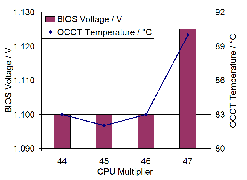
Despite being a relatively small company, EVGA have a very loyal following – the EVGA forums are full of like minded EVGA enthusiasts who enjoy the product range, particularly their graphics cards and motherboards. EVGA are often a little late to the market with a motherboard for the latest chipset due to their size or for extra planning, especially when they also build monster consumer products such as the EVGA SR-2 and SR-X, both dual socket products geared for performance. As part of this roundup, we have EVGA’s only Z77 motherboard on the market at the minute, the Z77 FTW.
EVGA Z77 FTW Overview
FTW is a fairly common internet acronym to mean ‘for the win’, and this is EVGA’s philosophy for a lot of their products, which are ultimately sold to gamers and overclockers. The EVGA Z77 FTW is a good looking board, with some extra features such as dual 8-pin CPU power connectors, an extra SATA controller, dual GbE network ports, PCIe disabling buttons, triple BIOS functionality and the PLX PEX 8747 chip, but not a lot else. EVGA’s tactic is the way their PLX chip is routed through the system, as shown by the diagram below:
Unlike other motherboards in this review, here we have eight lanes from the CPU going direct to the first PCIe slot, and the other eight go to the PLX via a multiplexer. If the PLX is in operation the multiplexer sends the second set of eight lanes to the PLX, otherwise it remains full bandwidth to the first PCIe. This results in the PLX having only 8 lanes worth of bandwidth upstream while providing 32 lanes downstream, a potential bottleneck.
In full four-GPU mode, this gives us x8/x16/x8/x8, technically a higher lane count overall, but these last three PCIe slots are limited to a total 8 lanes upstream bandwidth. EVGA state that this is not really an issue in gaming, as most communication between GPUs is via the SLI / CFX bridges, and that this setup should prove more beneficial to single GPU gamers than other PLX chip users.
My argument is that while it does increase single GPU bandwidth to non-PLX boards, single GPU users are ending up paying another $40 BOM cost for the PLX which they are not going to use? EVGA have informed me via email that the solution used by other manufacturers will always be worse in gaming for single and to a smaller extent dual GPU users compared to their solution above.
Unfortunately testing this hypothesis is a little distorted. The EVGA Z77 FTW unfortunately did not like my memory testing kit for these reviews, a G.Skill 16GB DDR3-2400 9-11-11 memory kit. Like the Biostar TZ77XE4 I reviewed a little while ago, and the ECS Z77H2-AX tested in this roundup, we had to run the memory at a slightly reduced setting, as neither the XMP nor automatic settings wanted to engage properly. As such, we were limited to DDR3-2000 9-11-11. Truth be told, this did not affect the results to a large degree, but the EVGA Z77 FTW also lacks MultiCore Enhancement, a ‘feature’ used by other manufacturers to run at 200 MHz more during full CPU loading. This double setback means that in certain circumstances, the EVGA might not perform as expected.
This is shown in our throughput benchmarks, where the EVGA is sometimes lingering to hold on to the rest of the pack. In contrast, our overclocking was quite good, with the EVGA Z77 FTW performing very well indeed. Users wanting an overclock beyond 4.6 GHz will have to adjust more options than on other boards, but the headroom is there as long as the CPU and cooling you are using can handle the temperatures.
EVGA software is limited, in that we only have EVGA ELEET at our disposal, and users will have to register on EVGA’s website to download the latest version. Unlike other boards in this price segment, we do not get WiFi functionality, mSATA, DVI/HDMI output, a graphical easy-to-understand BIOS, better-than-Realtek audio, or any small number of these, which puts EVGA down on the bang-for-buck impact. But for the money, there is a lot in the box, and EVGA warranty is direct with them rather than the retailer.
Update: EVGA state that the Z77 FTW will feature MultiCore Enhancement in a future BIOS update.
Visual Inspection
The first aspect a user may notice, aside from the fact this board is in an E-ATX form factor rather than ATX, is how relatively empty the CPU socket area feels. We have one large heatsink to the left, but it is outside the standard Intel specifications for socket area. EVGA clearly envisage users with large air coolers will be running this board, perhaps with a distinctive overclock. To top it off, there is also a pair of 8-pin CPU power connectors, for extreme overclockers to give the CPU more power.
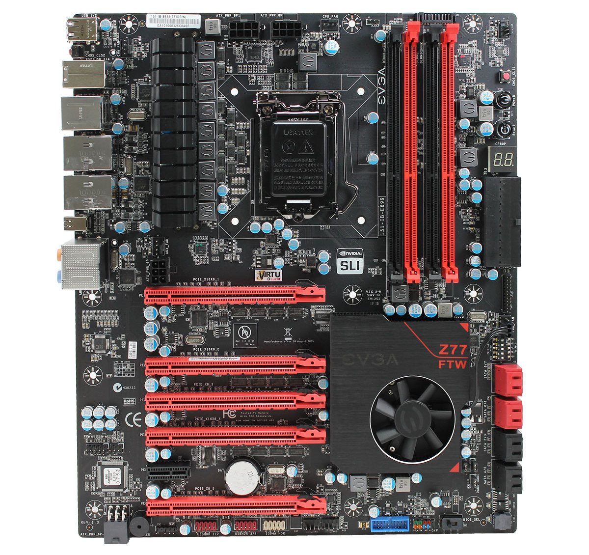
The socket area has access to four of the six fan headers on board – one 4-pin behind the IO panel at the top, one 4-pin just above the PCIe slots, the main CPU 4-pin beside the CPU power connectors, and another 4-pin at the top right of the motherboard. The other two fan headers, also both 4-pin, are found on the bottom of the board.
The memory slots use a single sided latch design, for easy insertion and removal (especially when space for hands is at a premium). Down the right hand side of the motherboard, EVGA start with a pair of power and reset buttons, with a ClearCMOS red button above followed by a two-digit debug display below. While not anything special when the motherboard is in a gaming rig, they do aid reviewers, extreme overclockers, and diagnosing faults alike. All the two-digit error codes are printed in the EVGA manual, and after boot this display doubles as a CPU temperature readout.
Underneath these, we find the 24-pin ATX power connector with an attachment to allow users to connect the cable parallel with the board. EVGA clearly have had requests from users for this, though I struggle to determine which market wants this – for users who will use this product inside a case, this provides them with the requirement for even more horizontal space to connect the cable. For overclockers, it would allow the 24-pin connector to remain out of the way.
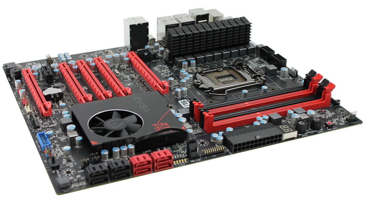
Going further down the right hand side, we have a JLCM header (presumably for EVGA diagnostics), a fan header in use by the chipset fan, and a series of PCIe disable switches. While not useful for the majority of users, these switches completely disable various PCIe slots to ensure that bandwidth is maximized to certain PCIe slots or for stability under sub-zero overclocking when not in use. The SATA ports are color coded, such that from the top we have two SATA 6 Gbps in red from a Marvell controller, two more SATA 6 Gbps in red from the chipset, and four SATA 3 Gbps in black also from the chipset.
One of EVGA’s main features is the triple BIOS system, which is located on the bottom right of the motherboard. Two of these BIOS chips are fixed to the board and the third is placed such that it is easy to remove and replace should a user ever scramble all three BIOSes at once. The onboard switch nearby helps to select between these BIOSes, and nearby there are also headers to switch the board into ‘dark mode’ (that is turning off all the LEDs).
On the south side of the board is our header array – two USB 2.0 headers, an IEEE1394 (FireWire) header, a USB 3.0 header and two fan outputs. Many of these headers are designed to work with the packaged rear brackets that come with the board, and by default these headers have rubberized protectors on them to prevent damage. On the far left of this board is a 6-pin PCIe power connector, to supply more power to the PCIe devices. Many of these headers can be compromised by a GPU in the fourth slot though.
The PCIe slots are designed such that GPUs are to be placed in slots 1, 2, 4 and 5; however any combination will work depending on the size of the cooler. In order to use any of the PCIe slots beyond the first however, power needs to be supplied either by the 6-pin PCIe power connector at the top of the PCIe, or at the bottom, or both if even more power is required for overclocking. This means that a user with a standard 4-GPU setup with each GPU requiring two 6-pin connectors, a total of 10 6-pin PCIe connectors is required, so choose a power supply wisely from the beginning. For our 4-GPU testing, I have two PSUs on hand to provide the power, and I was still stretching cables to get everything to fit.
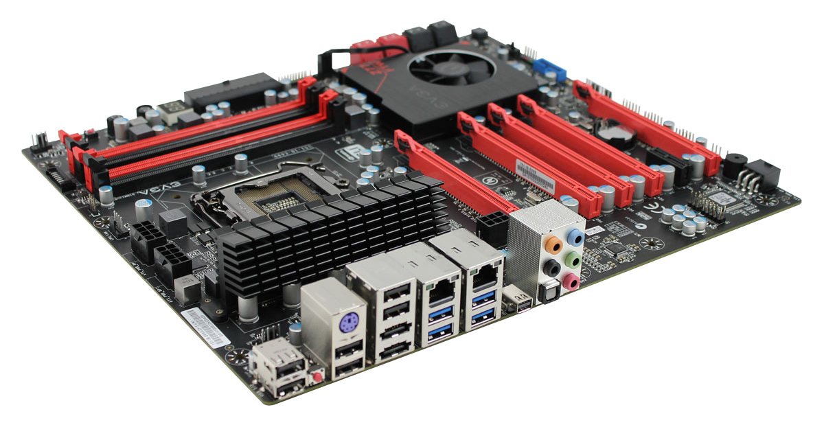
The rear panel is full of USB connections, as EVGA have decided to forgo any serious attempt at providing video outputs on the Z77 platform. From left to right we have two USB 2.0, a ClearCMOS button, a keyboard PS/2 port, four more USB 2.0 in black, two eSATA ports, dual GbE (Marvell), four USB 3.0 in blue, a DisplayPort connector (not to be confused with Thunderbolt), audio jacks and S/PDIF output. The DP connector would make sense if the board was bundled with a DP->HDMI connector (as a matter of personal preference as I have no DP monitors).
Board Features
| EVGA Z77 FTW | |
| Price | Link |
| Size | ATX |
| CPU Interface | LGA-1155 |
| Chipset | Intel Z77 |
| Memory Slots |
Four DIMMs, Supporting up to 32GB DDR3 1066-2133+ MHz, Non-ECC |
| Video Outputs | DisplayPort |
| Onboard LAN | Dual Marvell 88E8057 |
| Onboard Audio | Realtek ALC889 |
| Expansion Slots |
1 x PCIe 3.0 x16 (x8 if any other PCIe slot populated) 2 x PCIe 3.0 x16 (x8 if slot underneath is populated) 2 x PCIe 3.0 x8 1 x PCIe 2.0 x1 |
| Onboard SATA/RAID |
2 x SATA 6 Gbps (Intel), Supports RAID 0, 1, 5, 10 4 x SATA 3 Gbps (Intel), Supports RAID 0, 1, 5, 10 2 x SATA 6 Gbps (Marvell), Supports RAID 0, 1 |
| USB |
4 x USB 3.0 (Intel) [2 onboard, 2 back panel] 2 x USB 3.0 (Marvell) [2 back panel] 10 x USB 2.0 (Intel) [4 onboard, 6 back panel] |
| Onboard |
4 x SATA 6 Gbps 4 x SATA 3 Gbps 6 x Fan Headers 1 x USB 3.0 Header 2 x USB 2.0 Headers 1 x IEEE1394 Header Power/Reset Buttons Clear CMOS Button Two-digit Debug BIOS Switch |
| Power Connectors |
1 x 24-pin ATX Power Connector 2 x 8-pin CPU Power Connectors 2 x 6-pin PCIe Power Connectors |
| Fan Headers |
1 x CPU (4-pin) 1 x AUX (4-pin) 1 x CHA (4-pin) 3 x SYS (4-pin) |
| IO Panel |
6 x USB 2.0 4 x USB 3.0 2 x eSATA 1 x PS/2 Keyboard Port 2 x GbE 1 x ClearCMOS 1 x DisplayPort 1 x SPDIF Output Audio Jacks |
| Warranty Period | 3 Years |
| Product Page | Link |
The EVGA Z77 FTW has plenty of USB connectivity, with ten USB 2.0 ports and six USB 3.0 ports available, coupled alongside dual network ports, and six fan headers. Overclockers get the PCIe disable switches and dual 8-pin CPU power connectors, as well as the BIOS switch. However it does feature a lack of video outputs (DP only) compared the other motherboards, as well as the worst audio codec (Realtek ALC889) in comparison.
EVGA Z77 FTW BIOS
There are a very few companies who have yet to make the switch from a plain interface BIOS to the new wave of graphical interaction. EVGA is in this boat – while their BIOS is technically a UEFI, it still relies on keyboard controls and simple menu selections in order to get the options correct. Any semblance of an easy screen for all the basic information and/or fan controls are out of the window here, users have to explore to find the options they want, alongside a ton of options to which I have no clue what they do.
It should be noted at this juncture that the BIOS for the EVGA Z77 FTW currently follows Intel specifications for CPU Turbo implementation, such that for an i7-3770K we have 39x/39x/38x/37x multipliers for 1/2/3/4 core loading. Some other motherboard manufacturers use what ASUS call ‘MultiCore Enhancement’, which gives 39x/39x/39x/39x multipliers under the respective loading for better performance at the expense of increased heat, temperature, and potential longevity. EVGA will be implementing this feature in a later BIOS, however for our review we were locked into BIOS 1.07, the latest available on the EVGA website at the time of testing.
I would also like to note that the BIOS does not have a print screen function, so I apologize in advance for the potential poor quality of the upcoming BIOS images taken with a cheap $600 DSLR without a tripod.
Our first BIOS screen, while not graphical, contains the wealth of information I would expect from every manufacturer on the market. We have access to the BIOS version and build date, the processor being used as well as speed and cores/threads, memory speeds and amounts, and voltages/temperatures of the important components of the motherboard. Despite not being the most well presented set of information possible, it does satisfy the criteria needed by system builders, integrators and debuggers without needing to open the system and pry the CPU cooler off / install an operating system.
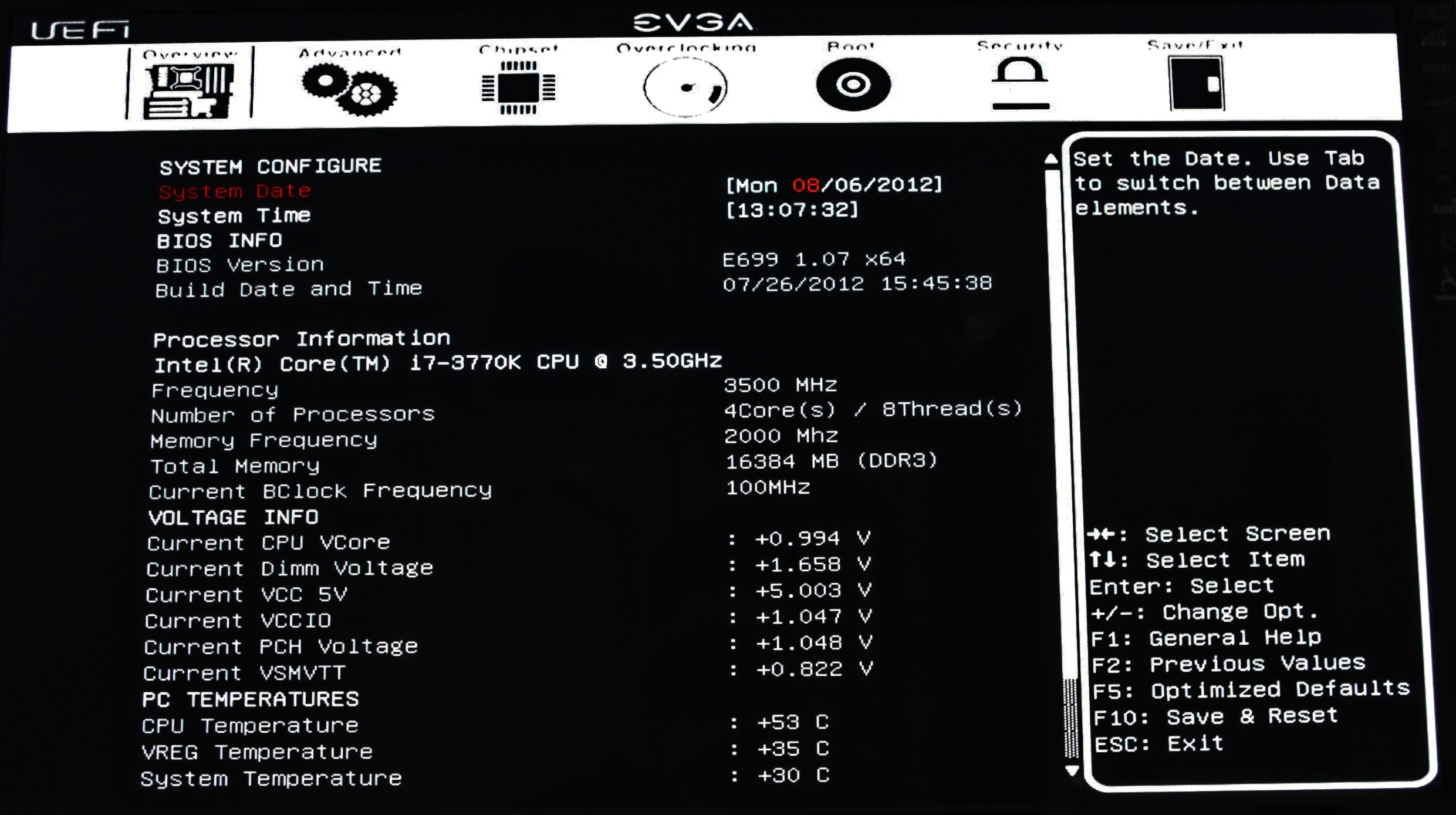
As long as the BIOS is updated from the early betas, we get a system which enables AHCI for the SATA ports by default, which is always beneficial. Unwanted controllers can be disabled through one of the ‘Onboard Devices’ sub-menu under ‘Advanced’. The EVGA Z77 FTW POST time benefits a great deal if the Marvell SATA controllers are unused, dropping from 19.55 seconds to 11.21 seconds when everything is disabled.
Fan controls are found under the ‘Advanced’ menu. We have access through the BIOS to a complex multi-point fan control system (no mention of gradients) that allows users to select a direct correlation between temperatures and fan speeds under the CPU header. Unfortunately this control is not provided through software as well, which is a shame given that these controls outshine some of the ones provided by top-tier manufacturers.
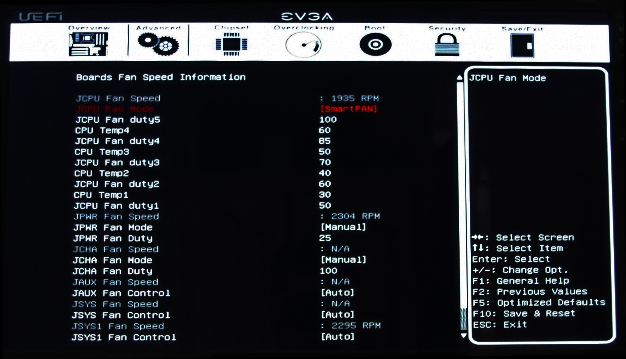
EVGA has a history of overclocking records – not surprising, as they have had on staff over the years some of the world’s most famous extreme overclockers, including Vince ‘Kingpin’ Lucido and Tsemenko ‘TiN’ Ilya. So when it comes to the overclocking section of their top line Z77 motherboard, we might expect some fantastic new features to help.
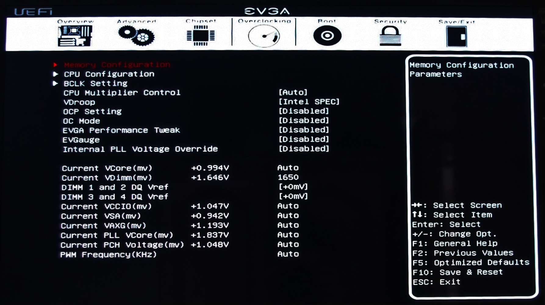
On the first main screen we get all the important CPU options – CPU multiplier control, LLC (VDroop) control, OCP (Over-Current Protection), Performance Teaks, and important CPU and system voltages. One feature worth explicitly mentioning is the OC Mode option – this is ideal for competitive overclockers, as it automatically disables all non-essential controllers on board to maximize stability. I like this feature.
Memory options are found in the ‘Memory Configuration’ menu, which give access to apply XMP profiles, or manual settings across the ranges. EVGA tell me that they have recently been working hard to ensure that XMP functionality will work across a wide range of kits, however my aggressively timed memory kit (DDR3-2400 9-11-11) that I use for Z77 reviews failed to register, neither would it work with additional VTT voltage. As a result, we had to run the kit at DDR3-2000 9-11-11 for our testing, which is not much of a difference in our testing suite.
C-State options are under the CPU configuration menus, and the BCLK adjustment is performed through its own menu. BCLK adjustment could easily be moved into the main OC menu with the multiplier adjustment, and my attempts at manipulating the BCLK heavily were not that successful – while most motherboards will happily boot with 108 MHz on my i7-3770K, the EVGA board was happy only at 104 MHz. I am unsure as to why this is the case, when I have seen results for the Z77 FTW hitting 108 MHz+.
The EVGA BIOS also comes with Boot Override, allowing for a single-time boot from specified device.
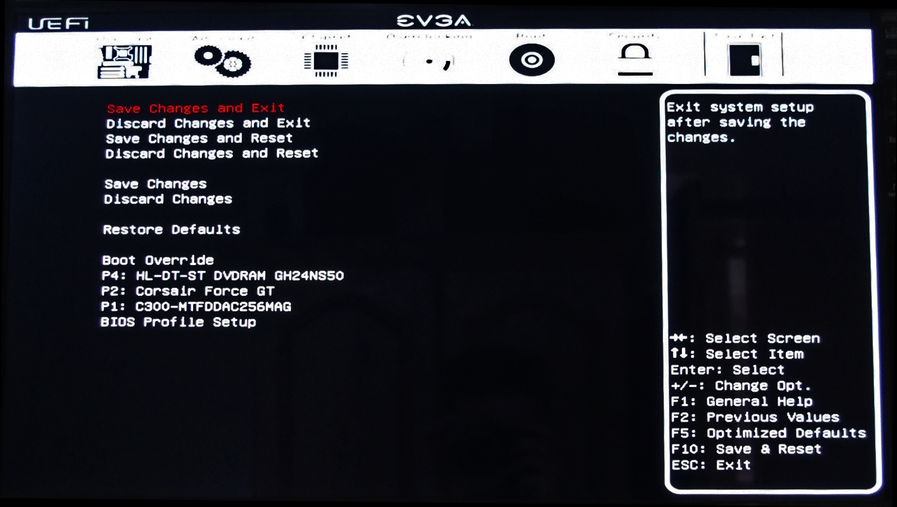


EVGA Z77 FTW Software
Given that EVGA is relatively small company in the motherboard arena, they suffer a similar fate when it comes to driver install programs when compared to companies in a similar position. While the install disk seems aesthetically nice with a supposed one button install, in actual fact the user must be present to accept all the menu options to install each of the drivers. The major top tier manufacturers perform silent install options, available with most of the generic driver installs (Realtek et al.), and so it is a small wonder why they are not applied here. With regards software, the sole application, ELEET, is not installed with the drivers but separately though the ‘next’ menu on the install CD.

ELEET
The sole software program provided by EVGA on the Z77 FTW is the Eleet Tuning Utility. This for most intents and purposes is a glorified CPU-Z with an EVGA skin, with a few small extras. The first screen is identical to CPU-Z in that regard, showing all the CPU information.
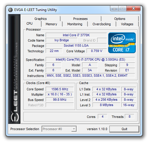
Where Eleet differs from CPU-Z is in a few of the EVGA specific options, such as the monitoring screen which shows temperatures, voltages and fan speeds. Unfortunately with Eleet we do not get any form of fan controls, despite the fact that the fan options in the BIOS were quite verbose.
Also at hand with Eleet is an overclocking menu, which allows users to adjust the multipliers and the BCLK. However the version I was supplied on the Driver Disk was not applicable for Z77 or Ivy Bridge – users will have to register online with EVGA and download the latest version of Eleet in order to get it to work, otherwise the following screen will be shown:
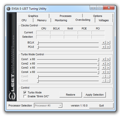
Users will also have to enable ELEET in the OC menu in the BIOS for this option to function.
One of the more interesting features with ELEET is again for the overclocking crowd, by providing an on-the-fly affinity adjuster. This allows with a keypress the ability to modify how many CPU threads a program is using. In the world of competitive overclocking, we require benchmarks to have the top priority on the CPU cores to get the best scores, which is where this area of the program will help.


Overall, the software from EVGA is not that special for a regular user, and without any serious fan controls or GUI based BIOS update utility is lacking in significant substance.
EVGA Z77 FTW In The Box
In EVGA boxes I have looked at in the past, there is a common theme of bundling as much in as you can. A lot of the extras in the box come in EVGA branded packaging, often individually sealed. This begs the question of how much this ‘individualization’ brings to the package as a whole, how much it costs to the consumer, and if it is necessary. Would I care if my additional SATA cables were in an EVGA branded plastic packet, or a non-descript see-through plastic packet? Nevertheless, there is a lot for your money with the Z77 FTW:
Driver Disk
Quick Start Manual
Quick Start Poster
Rear IO Shield
Four SATA Cables
2-GPU Flexi SLI Bridge
3-GPU Rigid SLI Bridge
SATA Power Cable (2 SATA to Molex)
IEEE1394 Bracket
Four-port USB 2.0 Bracket
Two-port USB 3.0 Bracket
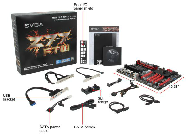
Aside from the packaging, the elements that stand out are the additional rear brackets provided. This motherboard is geared up to take four GPUs, and thus leave no space for rear brackets. However no four-GPU SLI connector is provided – the ideal situation is thus a dual GPU system and the brackets can fit in the additional slots. These brackets also cover all the main headers on the bottom of the board, for completeness.
Voltage Readings
After my first publication of OCCT voltage readings, a few readers responded with a more in-depth reasoning behind some of the results we were seeing. With this in mind, I would like to re-describe what we are doing with this test, and how it comes about.
Much of what an enthusiast overclocker does is monitor CPU temperature and voltage. Whatever settings a user places in the BIOS or OS is at the mercy of the motherboard - in terms of actually setting the values and reporting the values back. As an enthusiast, we have to rely on what readings we get back, and hope that motherboard manufacturers are being honest with their readings.
Take CPU voltage. What we as a user see in CPU-Z or OCCT is a time-averaged value that hides voltage ripple (if any) for power delivery. It is very easy for a motherboard manufacturer to hide this value, or to disregard slight deviations and report a constant value to the user. The CPU voltage reading can be taken at a variety of places on the power plane, which can vary between motherboards and manufacturers, meaning that each reading is essentially not comparable with the other. Nevertheless, as an enthusiast, we will constantly compare value A with value B.
Whether or not I can achieve 4.7 GHz with 1.175 volts on a particular board is inconsequential - your motherboard may perhaps produce the same result with a reading at 1.200 volts. The only way to test the actual value is with consistent methodology is via an oscilloscope connected to similar points on each board. This may sound like taking an OCCT reading is therefore redundant.
However, motherboards have settings relating to load line calibration. As load is applied to the CPU, the voltage across the processor decreases (VDroop). Load Line calibration essentially attempts to control this level of droop, by increasing voltage when voltage drops are detected away from a fixed value. Manufacturers have different ideas on how to modify LLC with respect to load, or whether the level of modification should be controlled by the user. Some manufacturers offer the option at a variety of levels, such that overclockers can be sure of the applied setting (even if it increases peak voltage, as explained by AnandTech in 2007).
By doing a full load OCCT test, we are essentially determining both how aggressive the motherboard is reporting the CPU voltage under load and how aggressive load line calibration is performing (from the point of view of the user without an oscilloscope or DVM). If someone has one of the motherboards we have tested and you have a different one, variations in load voltage should describe the offset you may require for overclock comparisons.
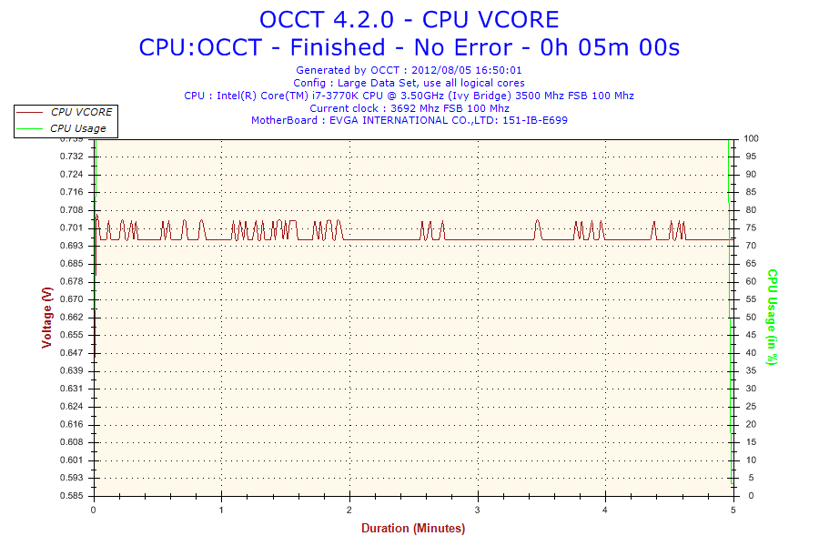
The EVGA Z77 FTW oddly has one of the lowest loading voltages reported by OCCT. This is also shown in CPU-Z, making the situation a little confusing as to whether this is a predetermined voltage offset scenario or the Load Line Calibration kicking in quite severely with an additional offset that is not reported.
EVGA Z77 FTW Overclocking
Note: Ivy Bridge does not overclock like Sandy Bridge. For a detailed report on the effect of voltage on Ivy Bridge (and thus temperatures and power draw), please read Undervolting and Overclocking on Ivy Bridge.
Experience with EVGA Z77 FTW
With no automatic overclock options, users are forced to use either the BIOS to adjust the CPU frequency, or an updated version of ELEET software from the EVGA website. Typically as an overclocker I jumped straight in with the BIOS.
The EVGA overclocking methodology is a little strange, albeit a bit simpler than some other implementations. All the important options such as the CPU multiplier and voltages are all contained within the main overclocking menu. There is even an ‘OC Mode’ option which disables all non-essential onboard controllers and ports to promote stability for competitive overclocking. Memory has its own menu, which allows for full adjustment of memory parameters, but for BCLK adjustment users have to navigate to a completely separate menu just for the single value.
With the pair of ClearCMOS buttons on board, recovering from a failed overclock that did not correct itself immediately was easy enough to do and implement again in the BIOS. If the system is not happy with the memory settings at boot time, the motherboard would produce the error code ‘55’ and beep several times to indicate this.
However memory can be a bit of an issue – I found that my kit would not perform at XMP. EVGA have said to me that memory is a priority right now and their board will work with the majority of standard mainstream kits.
When the more severe overclocks were being performed (4.6 GHz and above), the system would sometimes reduce the CPU multiplier automatically. I found that this is due to the power settings in the BIOS, which need to be raised. I personally set these at 250W (a value of 2000 as it takes values in 1/8 of a watt) and never had an issue, though without direct instructions do this seems a little odd.
Methodology:
Our standard overclocking methodology is as follows. We select the automatic overclock options and test for stability with PovRay and OCCT to simulate high-end workloads. These stability tests aim to catch any immediate causes for memory or CPU errors.
For manual overclocks, based on the information gathered from previous testing, starts off at a nominal voltage and CPU multiplier, and the multiplier is increased until the stability tests are failed. The CPU voltage is increased gradually until the stability tests are passed, and the process repeated until the motherboard reduces the multiplier automatically (due to safety protocol) or the CPU temperature reaches a stupidly high level (100ºC+).
Our test bed is not in a case, which should push overclocks higher with fresher (cooler) air. We also are using Intel's All-in-one Liquid Cooler with its stock fan. This is a 120mm radiator liquid cooler, designed to mimic a medium-to-high end air cooler.
Manual Overclock:
Our manual overclock testing was simple, starting at our standard 1.100 volts and 44x multiplier with Ivy Bridge. For stability we adjusted the VDroop in the BIOS to Disabled fairly quickly, and at higher multipliers the power limits of the CPU were adjusted to stop the system reducing the CPU multiplier. Here are our results:
At 44x, the BIOS was set to 1.100 volts on the CPU and VDroop left at Intel SPEC. In the OS this produced a memory error during PovRay. Thus VDroop was adjusted to ‘disabled’, which gave stability. The system showed 1.138 volts at load, with peak temperatures of 71°C during PovRay and 74°C during OCCT.
At 45x, the system was stable at a minimum BIOS voltage setting of 1.100 volts, which showed 1.126 volts in the OS at load. Peak temperatures observed were 72°C during PovRay and 73°C during OCCT.
At 46x, the system was stable at a minimum BIOS voltage setting of 1.125 volts, which showed 1.150 volts in the OS at load. Peak temperatures observed were 77°C during PovRay and 80°C during OCCT.
At 47x, the TDP limits for the CPU were raised to 250W. With this, the system was stable at a minimum BIOS voltage setting of 1.175 volts, which showed 1.197 volts in the OS at load. Peak temperatures observed were 82°C during PovRay and 84° during OCCT.
When attempting to reach 48x, the system was still not stable at 1.275 volts set in the BIOS, causing PovRay to hang the system after a couple of minutes and temperatures to rise above 100°C.
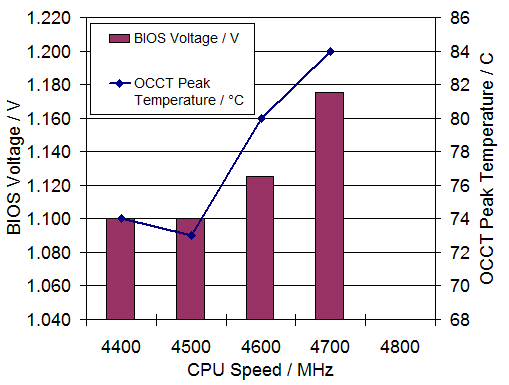
Many thanks to...
We must thank the following companies for kindly donating hardware for our test bed:
OCZ for donating the Power Supply and USB testing SSD
Micron for donating our SATA testing SSD
G.Skill for donating our memory kits
ASUS for donating AMD GPUs and some IO Testing kit
ECS for donating NVIDIA GPUs
Test Setup
| Processor |
Intel Core i7-3770K ES 4 Cores, 8 Threads, 3.5 GHz (3.9 GHz Turbo) |
| Motherboards |
ASRock Z77 Extreme4 ASRock Z77 Extreme6 ASRock Z77 Extreme9 ASRock Fatal1ty Z77 Professional ASUS P8Z77-V Pro ASUS P8Z77-V Deluxe ASUS P8Z77-V Premium Biostar TZ77XE4 ECS Z77H2-AX EVGA Z77 FTW Gigabyte GA-Z77X-UD3H Gigabyte GA-Z77X-UD5H Gigabyte GA-Z77MX-D3H Gigabyte G1.Sniper 3 MSI Z77A-GD65 |
| Memory | G.Skill F3-19200CL9Q-16GBZMD |
| Power Supply | OCZ 1250W Gold ZX Series |
| Cooling | Intel All-in-One Liquid Cooler |
| Hard Drive | Micron RealSSD C300 256GB |
| Optical Drive | LG GH22NS50 |
| Case | Open Test Bed - CoolerMaster Lab V1.0 |
| Operating System | Windows 7 64-bit |
| SATA Testing | Micron RealSSD C300 256GB |
| Thunderbolt Testing | LaCie Little Big 240GB |
| USB 2/3 Testing | OCZ Vertex 3 240GB with SATA->USB Adaptor |
Power Consumption
Power consumption was tested on the system as a whole with a wall meter connected to the OCZ 1250W power supply, while in a dual 7970 GPU configuration. This power supply is Gold rated, and as I am in the UK on a 230-240 V supply, leads to ~75% efficiency > 50W, and 90%+ efficiency at 250W, which is suitable for both idle and multi-GPU loading. This method of power reading allows us to compare the power management of the UEFI and the board to supply components with power under load, and includes typical PSU losses due to efficiency. These are the real world values that consumers may expect from a typical system (minus the monitor) using this motherboard.
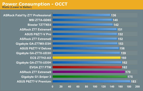
As a general rule, we see that the PLX 8747 motherboards consumer more power in most scenarios. The only exception to this is the EVGA Z77 FTW under Metro2033, which comes in at 480 W compared to the ASRock Z77 Extreme9 at 524 W.
POST Time
Different motherboards have different POST sequences before an operating system is initialized. A lot of this is dependent on the board itself, and POST boot time is determined by the controllers on board (and the sequence of how those extras are organized). As part of our testing, we are now going to look at the POST Boot Time - this is the time from pressing the ON button on the computer to when Windows starts loading. (We discount Windows loading as it is highly variable given Windows specific features.) These results are subject to human error, so please allow +/- 1 second in these results.
Both the ECS and EVGA motherboards offer big POST time gains when controllers are turned off, whereas the ASRock is very quick by default. The G1.Sniper 3 on the other hand gives us the slowest stripped time out of any motherboard tested.
Overclocks
Here at AnandTech we want to provide quick and easy ways to determine if a board is good for you (with in-depth analysis of course). So here is a quick round up of our overclocking results. Overclocks are tested for stability with PovRay and OCCT - while these may not be the most strenuous of stability tests, it does offer a quick check for memory errors under high load (and also balances testing time with getting the next board on for review!).
|
CPU Speed (MHz) |
BIOS Voltage (Volts) |
PovRay Peak Temp (ºC) |
OCCT Peak Temp (ºC) |
Notes | |
|
ASRock Fatal1ty Z77 Professional |
4700 | 1.200 | 89 | 89 | PLL Overvoltage enabled |
|
ASRock Z77 Extreme4 |
4700 | 1.175 | 86 | 86 | LLC Level 1 |
|
ASRock Z77 Extreme6 |
4700 | 1.175 | 81 | 82 | LLC Level 1 |
|
ASRock Z77 Extreme9 |
4700 | 1.200 | 92* | 94* |
*High Ambients LLC Level 1 |
|
ASUS P8Z77-V Deluxe |
4700 | 1.225 | 89 | 84 | PLL Overvoltage enabled |
|
ASUS P8Z77-V Pro |
4700 | 1.200 | 83 | 86 | PLL Overvoltage enabled |
|
ASUS P8Z77-V Premium |
4700 | 1.225 | 93 | 96 | High Ambients |
|
Biostar TZ77XE4 |
4700 | 1.180 | 84 | 85 | None |
|
ECS Z77H2-AX |
4700 | 1.125* | 87** | 90** |
*Odd VDroop Behaviour **High Ambients VDroop Disabled |
|
EVGA Z77 FTW |
4700 | 1.175 | 82 | 84 |
VDroop Disabled Power Limits Raised |
|
Gigabyte Z77X-UD5H |
4700 | 1.225 | 88 | 88 | LLC Extreme |
|
Gigabyte Z77X-UD3H |
4700 | 1.200 | 82 | 86 | LLC Extreme |
|
Gigabyte Z77MX-D3H |
4700 | 1.200 | 80 | 84 | LLC Extreme |
|
Gigabyte G1.Sniper 3 |
4700 | 1.200 | 85 | 88 | LLC Extreme |
|
MSI Z77A-GD65 |
4700 | 1.250 | 90 | - | PLL Overvoltage enabled |
System Benchmarks
USB Speed
For this benchmark, we run CrystalDiskMark to determine the ideal sequential read and write speeds for the USB port using our 240 GB OCZ Vertex3 SSD with a SATA 6 Gbps to USB 3.0 converter. Then we transfer a set size of files from the SSD to the USB drive using DiskBench, which monitors the time taken to transfer. The files transferred are a 1.52 GB set of 2867 files across 320 folders – 95% of these files are small typical website files, and the rest (90% of the size) are the videos used in the Sorenson Squeeze test.
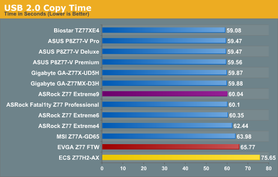
The obvious outlier in what should be a relatively simple USB 2.0 test is the ECS Z77H2-AX. For some unknown reason, it suffers a limited USB 2.0 speed at a round 25 MBps either read or write. To a certain extent, the EVGA also has some problems in USB 2.0 write.
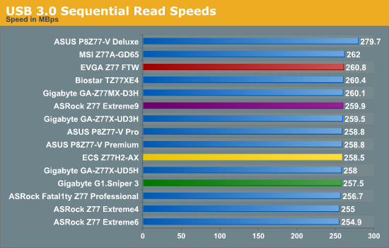
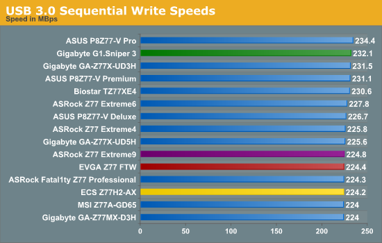
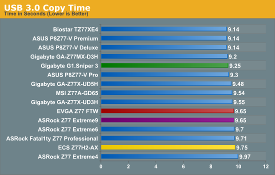
The USB 2.0 problems are not present at all in USB 3.0 testing, with each of the boards performing similarly.
SATA Testing
We also use CrystalDiskMark for SATA port testing on a C300 drive. The sequential test (incompressible data) is run at the 5 x 1000 MB level. This test probes the efficiency of the data delivery system between the chipset and the drive, or in the case of additional SATA ports provided by a third party controller, the efficiency between the controller, the chipset and the drive.
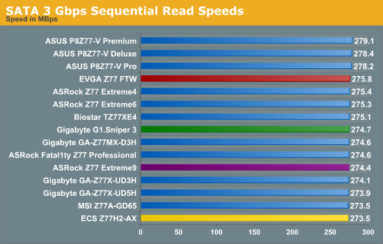
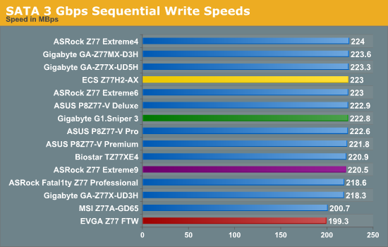
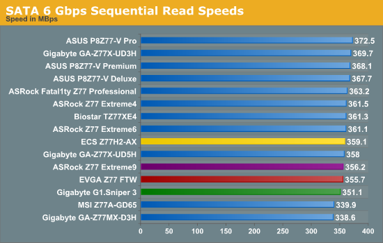
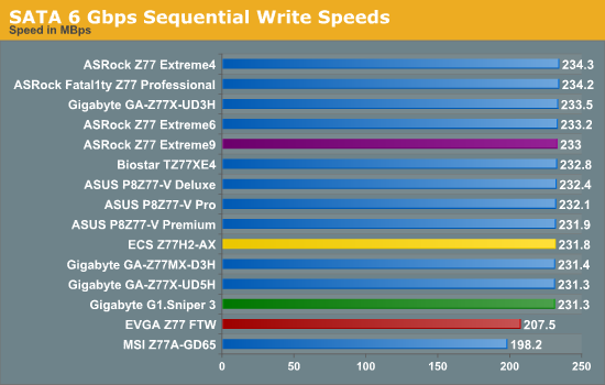
The EVGA Z77 FTW motherboard has issues in SATA write tests, similar to the MSI previously tested.
DPC Latency
Deferred Procedure Call latency is a way in which Windows handles interrupt servicing. In order to wait for a processor to acknowledge the request, the system will queue all interrupt requests by priority. Critical interrupts will be handled as soon as possible, whereas lesser priority requests, such as audio, will be further down the line. So if the audio device requires data, it will have to wait until the request is processed before the buffer is filled. If the device drivers of higher priority components in a system are poorly implemented, this can cause delays in request scheduling and process time, resulting in an empty audio buffer – this leads to characteristic audible pauses, pops and clicks. Having a bigger buffer and correctly implemented system drivers obviously helps in this regard. The DPC latency checker measures how much time is processing DPCs from driver invocation – the lower the value will result in better audio transfer at smaller buffer sizes. Results are measured in microseconds and taken as the peak latency while cycling through a series of short HD videos - under 500 microseconds usually gets the green light, but the lower the better.
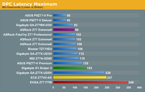
A trend worth noting is that all PLX PEX 8747 motherboards have some additional DPC latency compared to their brethren. Any score below 500 microseconds is good, but under 200 microseconds is better. The EVGA and the ECS fall outside this region with the two worst DPC scores on Z77. The best of the boards tested in this roundup comes with the ASRock Z77 Extreme9.
3D Movement Algorithm Test
The algorithms in 3DPM employ both uniform random number generation or normal distribution random number generation, and vary in various amounts of trigonometric operations, conditional statements, generation and rejection, fused operations, etc. The benchmark runs through six algorithms for a specified number of particles and steps, and calculates the speed of each algorithm, then sums them all for a final score. This is an example of a real world situation that a computational scientist may find themselves in, rather than a pure synthetic benchmark. The benchmark is also parallel between particles simulated, and we test the single thread performance as well as the multi-threaded performance.
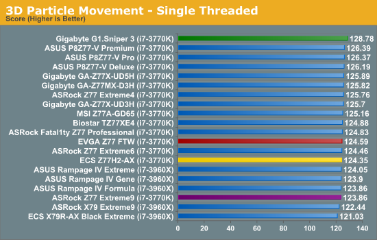
The motherboards we have today fit into two extremes in single threaded performance – the difference being up to 300 MHz in MT from the ASRock Z77 Extreme9 (scoring 123.86 in 3DPM) and the Gigabyte G1.Sniper 3 (scoring 128.78). Due to the extra MHz of the G1.Sniper 3, it takes many of our Z77 records.
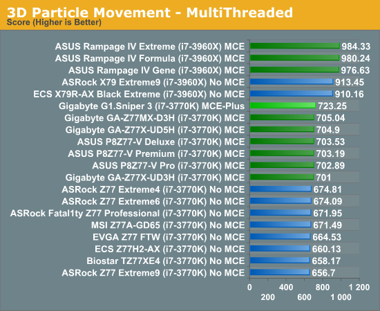
The difference in speed is more pronounced in the multithreaded version, where the weaker algorithms that define CPU speed are pointed out. The difference between the ASRock and the Gigabyte is an astonishing 10% of the ASRock score, which is not all down to pure MHz.
WinRAR x64 3.93 - link
With 64-bit WinRAR, we compress the set of files used in the USB speed tests. WinRAR x64 3.93 attempts to use multithreading when possible, and provides as a good test for when a system has variable threaded load. If a system has multiple speeds to invoke at different loading, the switching between those speeds will determine how well the system will do.
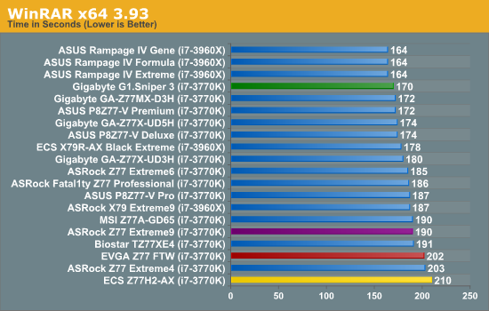
With the WinRAR test, the Gigabyte takes the lead by two seconds from any other Z77 board. Unfortunately the rest end up at the bottom, some 20-30 seconds slower.
FastStone Image Viewer 4.2 - link
FastStone Image Viewer is a free piece of software I have been using for quite a few years now. It allows quick viewing of flat images, as well as resizing, changing color depth, adding simple text or simple filters. It also has a bulk image conversion tool, which we use here. The software currently operates only in single-thread mode, which should change in later versions of the software. For this test, we convert a series of 170 files, of various resolutions, dimensions and types (of a total size of 163MB), all to the .gif format of 640x480 dimensions.
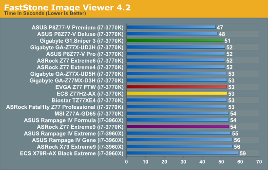
In comparison to previous results, ASUS seem to have a more adaptive single threaded algorithm when it comes to our FastStone test. The Gigabyte still does well, with the rest of the field only a few seconds back.
Xilisoft Video Converter
With XVC, users can convert any type of normal video to any compatible format for smartphones, tablets and other devices. By default, it uses all available threads on the system, and in the presence of appropriate graphics cards, can utilize CUDA for NVIDIA GPUs as well as AMD APP for AMD GPUs. For this test, we use a set of 32 HD videos, each lasting 30 seconds, and convert them from 1080p to an iPod H.264 video format using just the CPU. The time taken to convert these videos gives us our result.
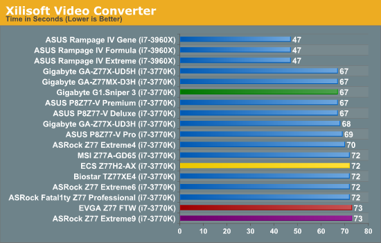
Converting videos is all about speed, and as such the Gigabyte joins the other MCE enabled boards but is unable to pull ahead. The other boards in this review are some 5-6 seconds behind.
x264 HD Benchmark
The x264 HD Benchmark uses a common HD encoding tool to process an HD MPEG2 source at 1280x720 at 3963 Kbps. This test represents a standardized result which can be compared across other reviews, and is dependant on both CPU power and memory speed. The benchmark performs a 2-pass encode, and the results shown are the average of each pass performed four times.
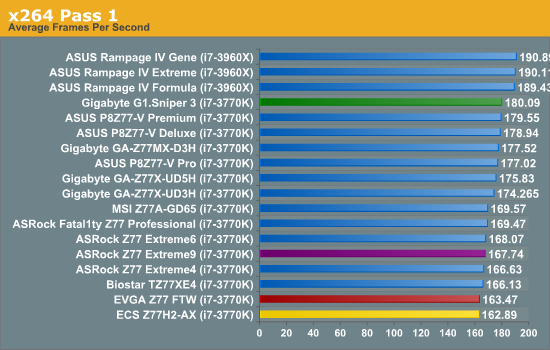
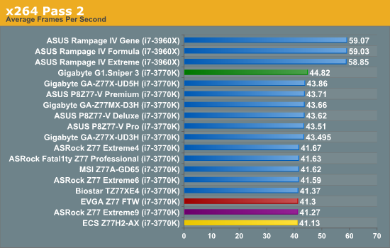
Gaming Benchmarks
Clarification of Lane Counts
In this review, we are dealing with motherboards that utilize the PLX PEX 8747 chip differently, such that the PCIe lanes that power each of these boards can come from either the CPU or the PLX chip depending on routing. The following describes the behavior of the four motherboards in this review, along with the ASUS P8Z77-V Premium reviewed previously that also utilized the PLX chip.
ASUS: 16x CPU to PLX, x8/x8/x8/x8
Gigabyte: 16x CPU to PLX, x8/x8/x8/x8
EVGA: 8x CPU to PCIe 1, 8x CPU to PLX for overall x8/x16/x8/x8
ASRock: 16x CPU to PLX, x8/x8/x8/x8
ECS: 16x CPU to PLX, x16/x8/x8
Dirt 3
Dirt 3 is a rallying video game and the third in the Dirt series of the Colin McRae Rally series, developed and published by Codemasters. Using the in game benchmark, Dirt 3 is run at 2560x1440 with full graphical settings. Results are reported as the average frame rate across four runs.
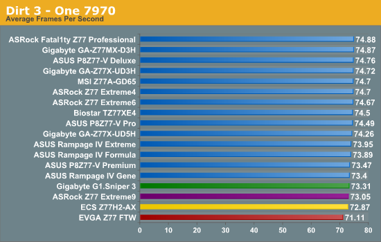
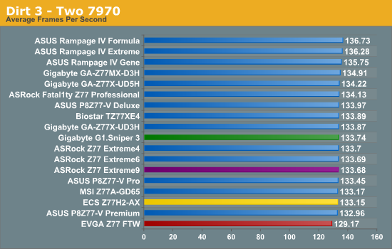
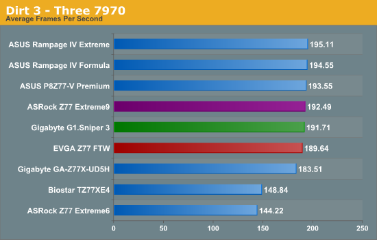
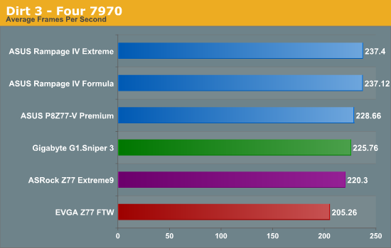
Despite the lane adjustment for EVGA to improve single GPU performance over the other boards, this does not materialize in Dirt3 which ends up being very power and memory hungry. When looking at a fully loaded setup, the eight lane uplink from the EVGA looks to be a limiting factor also.
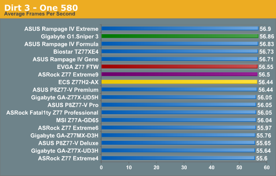
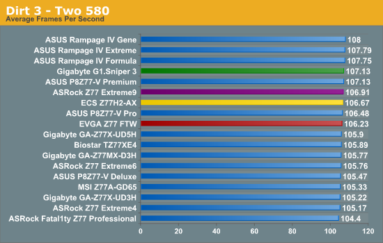
In comparison, there does not seem to be much to stretch apart the motherboards when NVIDIA cards are used.
Metro2033
Metro2033 is a DX11 benchmark that challenges every system that tries to run it at any high-end settings. Developed by 4A Games and released in March 2010, we use the inbuilt DirectX 11 Frontline benchmark to test the hardware at 2560x1440 with full graphical settings. Results are given as the average frame rate from 10 runs.
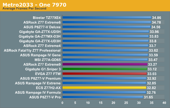
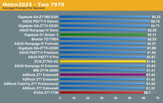
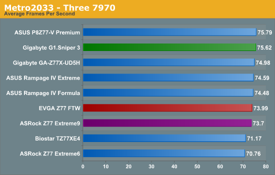
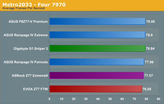
For single card setups in Metro2033, the routing via the PLX produces a 4.7% to 6.2% difference in frame rates compared to the top results.
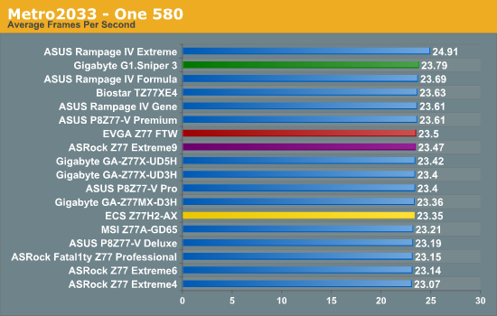
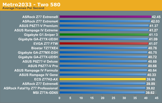
Whereas for NVIDIA cards, Metro2033 shows indifference between PLX enabled motherboards and non-PLX motherboards.
Conclusion: Gigabyte G1.Sniper 3
The Gigabyte G1.Sniper 3 has followed the trend of its sister, the Z77X-UD5H (I say sister rather than brother because they are ‘mother’ boards, right?). The key to getting a good motherboard on market is to make it perform well, and then make it feel like it is good value. Not only is it imperative that you try and undercut the competition, but the package must be complete in comparison to the other boards you are being compared to.
This is what the G1.Sniper 3 does for $280. We have a package that includes the PLX PEX 8747 solution for multiple GPUs, a gaming network port from Qualcomm Atheros in the Killer 2201-B alongside an Intel NIC, ten USB 3.0 ports, ten SATA ports, all the video outputs on the IO, some legacy in the PS/2 and IEEE1394 connectivity, and a TPM for business users. Inside the box we have a plethora of SATA cables, along with a USB 3.0 bracket, WiFi card, antenna, an eSATA bracket with cables and a pair of SLI bridges.
Where the G1.Sniper 3 ends up being very sneaky is in terms of the default speed the CPU is set to run at. Currently ASUS and Gigabyte motherboards run a feature that ASUS call Multicore Enhancement, which means instead of running at 39x/39x/38x/37x at 1/2/3/4 core load for an i7-3770K, they will run at 39x/39x/39x/39x. The Gigabyte G1.Sniper 3 goes one further, in this case making the CPU run one multiplier above the maximum turbo bin – in this case 40x/40x/40x/40x. As a result, the G1.Sniper 3 takes effectively a clean sweep in all our 2D testing which requires most heavily on the CPU and memory. For your money, Gigabyte has provided an out-of-the-box overclock which will beat the competition, on the understanding that it technically breaks your CPU warranty (and probably the motherboard warranty as well). Not that they advertise this of course – it all comes out in the reviews though.
My take on this situation has varied over the past few chipsets where MultiCore Enhancement has been a factor. In X79, I disabled it and made the board run at Intel specifications. Then I realized that users will most likely run these boards at stock, so it is up to the manufacturer as to how adventurous they want their default settings to be, much in the same way manufacturers may provide aggressive memory settings. With Gigabyte taking it to a new level, I will still operate under the circumstance that it is a ‘feature’ – Gigabyte are clearly willing to take the inherent risk in their product.
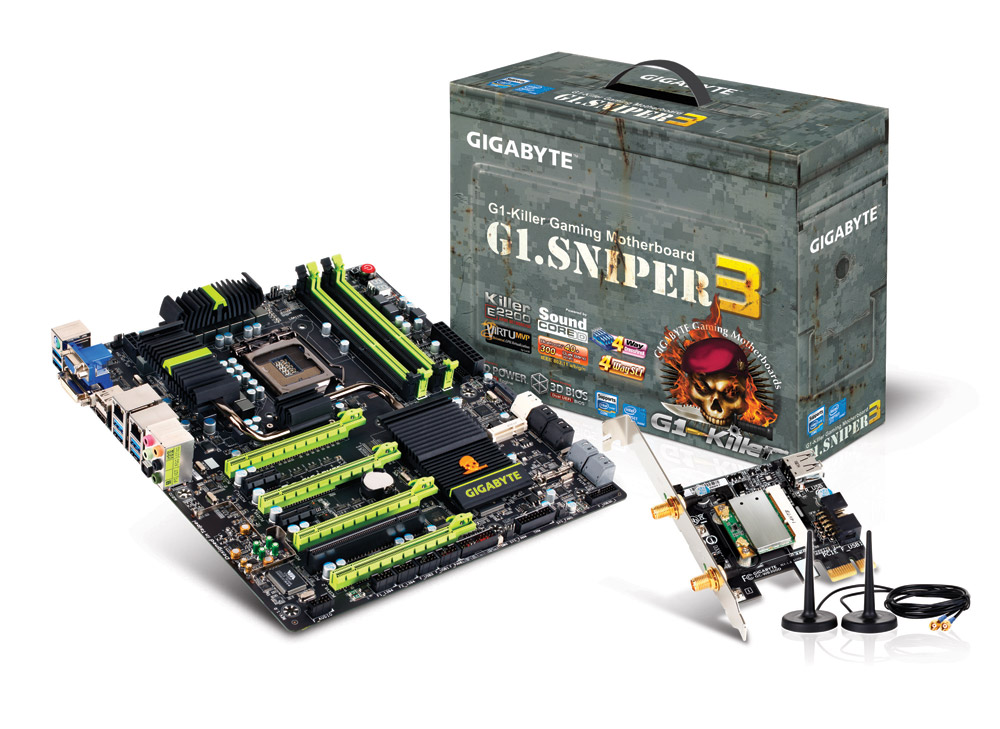
This extra enhancement on the CPU translates in certain GPU tests as well, which will be good to the ears of gamers. Overclocking on the G1.Sniper 3 mirrored what we have achieved with other Z77 boards, as with Ivy Bridge our temperature limitations really kick in due to voltages above 1.2 V.
If Gigabyte were to be brought down by an area of the package, it would be the eternal issue of their software and fan controls, which have remained stagnant over the past 18 months or so. I do hope that they give a fresh injection to R&D to develop the potential of the software, and combine this with a bit more money in the fan headers, as Gigabyte’s main competitor has this tied up and in the bag for now.
It is easy to recommend the Gigabyte G1.Sniper 3 – for the price it provides the performance, the functionality and the extras in the box that a user needs. Somehow Gigabyte has been able to undercut the competition to good effect, and passing this good value package onto consumers. There are of course some rough edges as with any product, but out of this roundup it would be the Gigabyte I would recommend for most usage scenarios that require the PLX PEX 8747.
With this in mind, I would like to give the Gigabyte G1.Sniper 3 the AnandTech Editors Choice Bronze Award. For price, performance, and the sense of a good value package, the G1.Sniper 3 offers one of the best price competitive PLX PEX 8747 packages available today.

Editors Choice Bronze Award
Gigabyte G1.Sniper 3
Conclusion: ASRock Z77 Extreme9
The ASRock Z77 Extreme9 comes in following a good performance from the G1.Sniper 3. This is compounded by the fact that the ASRock motherboard comes in as the most expensive motherboard in this roundup, some $70 more than the Gigabyte at $350. Any way you slice it, $350 is a lot of green to be laying down for a Z77 motherboard.
For the cash, ASRock offers a straight forward 4-way GPU setup. As part of the additional functionality, we have access to a total of 10 SATA ports (six SATA 6Gbps) and 12 USB 3.0 ports, more than any other product. The only video output onboard is HDMI, which contributes to the extra space in the IO panel being filled with USB, IEEE1394, and eSATA. For this price we also get dual gigabit Ethernet from Broadcom controllers, with the added bonus that can be teamed. If that was not enough networking functionality, we also have an integrated WiFi card from a mPCIe slot, and a dual receive/transmit antenna box which fits into a large drive bay slot.
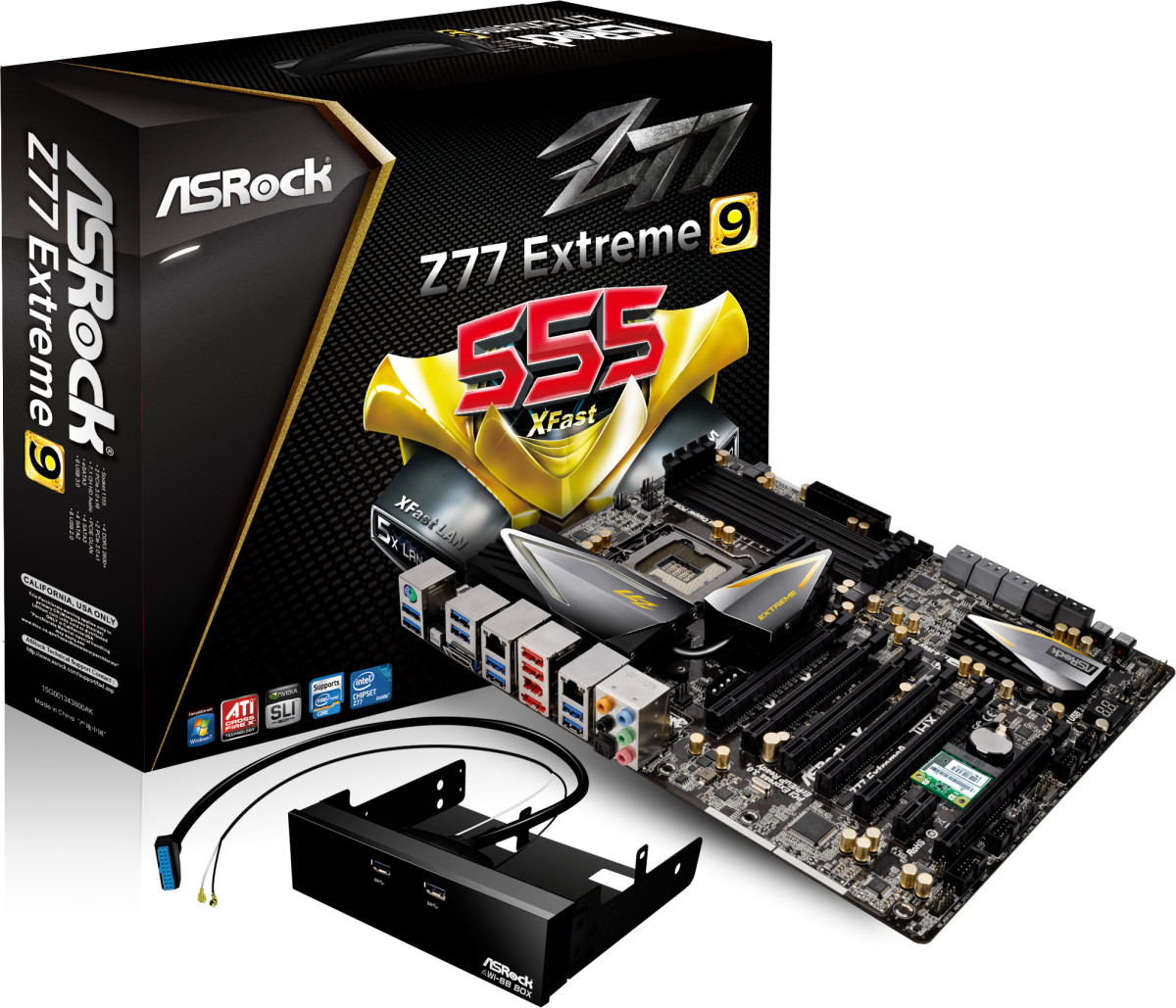
When examined in isolation, the Z77 Extreme9 would come across as a nice board to play around with – the BIOS is easy to navigate, and the combination of XFast USB, XFast LAN and XFast RAM offer a good software package. But in comparison to other products on the market, it is let down by the not-so-great fan controls, the use of only a Realtek ALC898, no Intel NICs, and the performance at stock settings.
While the ASRock took like a fish to water with my tight memory XMP profile, the same cannot be said for the benchmark results. ASRock had ample time before my review to release a public BIOS with MultiCore Enhancement, giving the CPU increased performance at heavy loading in exchange for heat and power consumption. However they did not, and the Z77 Extreme9 actually has a poor multithreaded showing.
Much of the CPU performance is moot if you overclock, and the ASRock has a few automatic overclock settings which work straight away. Overclocking options for manual adjustment are readily available to the user in a single screen. ASRock have a BIOS update planned which modifies the look of the BIOS a little in the near future.
ASRock have unfortunately been caught unawares by the competition, which have both undercut them in terms of price and value. The Z77 Extreme9 would have to price match the G1.Sniper 3 in order be the slightest bit competitive in terms of value – then the question of performance may rear its head. ASRock also have the Z77 OC Formula in the wings, which may solve some of these issues, although it is aimed more at aggressive and competitive overclockers.
Conclusion: ECS Z77H2-AX
The ECS Z77H2-AX comes straight out of the box in a bedazzling gold sheen. If you want a gold colored motherboard and do not feel like spray painting heatsinks and capacitors yourself, then the ECS Z77H2-AX has you covered. It is just a shame that the rest of the package does not live up to that expectation.
If we start from the top, we have a PLX PEX 8747 motherboard that is retailing at the time of writing on Newegg for $310. The ECS Z77H2-AX offers something a little different than the other motherboards such that instead of having four full-length PCIe slots for multiple GPU action, ECS have gone down to three (which takes it away from a very small minority of users) and thus x16/x8/x8 connectivity. With this setup, we get space between the first and second full sized GPU, or space for two three-slot GPUs in an x16/x16 configuration.
On board we get built in WiFi and Bluetooth, as well as an mSATA port and the first motherboard in our Z77 reviews to use a Texas Instruments branded USB 3.0 controller. Unfortunately, the buck stops there.
The system uses only six of the twelve USB 2.0 ports supported by the chipset, and only six USB 3.0 total compared to other motherboards in this review that offer up to twelve USB 3.0. We have access to six SATA ports on board and an mSATA, where ECS decide to leave one of the SATA ports supported by the chipset unconnected. To save costs we have a Realtek combination of NIC and Audio, but even then we only get the ALC892 audio rather than the ALC898. The ECS Z77H2-AX has only one NIC, rather than the other motherboards in this review which have two each. For video outputs, we get VGA and HDMI, which remove the use of any display above 1920x1200 due to Ivy Bridge limitations.
In terms of performance, ECS have decided not to go down the MultiCore Enhancement route. It goes a little further than that, in the sense that our multithreaded testing on the ECS Z77H2-AX seemed a little sluggish compared to some other boards. It should also be noted that our USB 2.0 sequential testing resulted in a 20% speed loss compared to every other Z77 motherboard we have ever tested. For our real world copy test this meant an increase from 60 seconds to 75 seconds.
Overclocking was a little unusual, with the motherboard offering its own interpretation of Load Line Calibration causing a positive bias on the CPU voltage when at load by as much as 0.075 volts. Nevertheless we did hit 4.7 GHz with ease. Memory on the other hand was a little tricky to navigate, with the motherboard refusing our XMP setting or any attempt to set XMP timings. In the end, we settled for testing on 2133 10-12-12 rather than 2400 9-11-11.
The BIOS needs a little work, particularly to correct the ClearCMOS issue and resetting to defaults, as well as adjusting the SATA configuration from IDE to AHCI by default. Also, the BIOS seems to manipulate the video output of the GPUs to the physically lowest card plugged in, which is also an unusual situation. We also cannot update the BIOS through the BIOS.
The software also needs polish, with the Live Update on the drivers and utilities not working properly. The one redeeming feature despite the lack of fan headers on board is the use of hysteresis on the fan header control, which I rather like.
For $310, the ECS Z77H2-AX is way out of its league. My gut feeling is that ECS have overpaid for the PLX chip, or are thinking that a lick of gold paint can bring in the big money. Even if it was brought down to $250, it would be a hard sell. In comparison to the Gigabyte Z77X-UD5H which retails at $180, the Gigabyte board runs rings around the ECS in functionality and benchmarks. Anyone that wants to argue otherwise has not compared the two.
Conclusion: EVGA Z77 FTW
EVGA is a brand that is often synonymous with high end products and a loyal fan base. With respect to motherboards, EVGA have produced some of the most creative and popular designs, especially in the X58 era with the EVGA SR-2, a dual socket motherboard for Xeon processors, and the X58 Classified. With a wealth of overclocking knowledge, the EVGA brand has also produced world records in overclocking.
When it comes to the Z77 platform, despite overclocking on Ivy Bridge being not as cut and thrust as some older platforms, EVGA still use that knowledge to produce a board that users can overclock on. As a result, we get some great overclocking options and a board that happily hits 4.7 GHz on our i7-3770K during testing in the Z77 FTW.
The main reason the EVGA Z77 FTW was included in this review is due to two factors – it comes in between the $280-$350 mark at $310, and also contains a vital PLX PEX 8747 chip, used for creating a wider range of PCIe lane opportunities than the standard Z77 chipset. EVGA take a different approach than the other manufacturers in our review, by only sending eight of the sixteen PCIe 3.0 lanes from the CPU to the PLX chip. This leaves the other eight to concentrate on the first PCIe slot, and should help single and dual GPU overclocking which can take a hit due to the PLX chip.
Users of multiple PCIe devices are advised to always keep the GPU in the first slot to maximize throughput, even if the system recognizes the electrically connected lane counts. While it sounds better to have x16/x16 from placing GPUs in slots two and four, keeping them in slots one and four (x8/x16) is actually preferential due to the eight lanes direct to the CPU that the first GPU has.
If that was not complex enough, we should also point out that the EVGA Z77 FTW does not include a form of MultiCore Enhancement using BIOS 1.07 or below. This feature on some other motherboards increases the CPU speed at heavier loading at the expense of power and temperature, but also increases their benchmarking scores a little. EVGA say that they will have this ‘feature’ in a later BIOS.
Our testing also took another hit, with the EVGA Z77 FTW taking the same policy as Biostar and ECS on their Z77 motherboards, by not liking our test memory kit at XMP. As a result, we had to run the system at DDR3-2000 9-11-11. The memory speed of a board does not affect the test bed to any significant degree, but coupled with the lack of MultiCore Enhancement means that out of the box, given the testing results, the EVGA does not keep pace with ASUS and EVGA even at stock speeds. This is shown quite dramatically during our 3DPM Multithreaded test, where the EVGA has a less than optimal multithreading turbo adjustment algorithm at play.
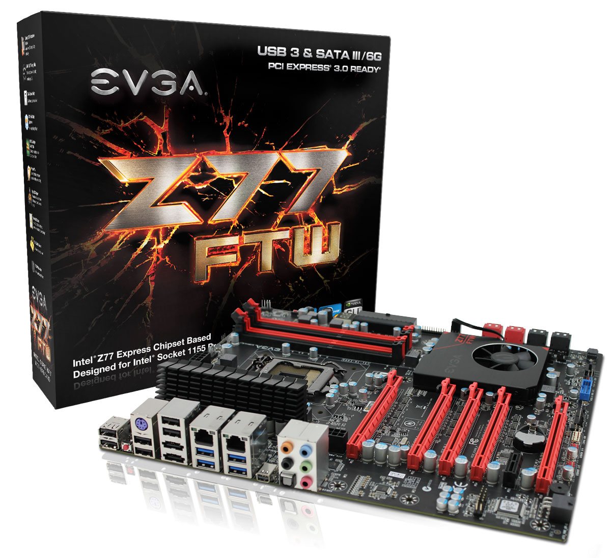
Feature wise, the Z77 FTW comes without the main video outputs, plunging for DisplayPort only, and in terms of extra features these are limited to a 24-pin ATX connector at right angles to normal, dual NIC, an extra SATA controller, access to three BIOS profiles, and a differently wired PLX chip. There is a lot in the box as well, especially if you like back panel connectors. Compared to the other motherboards in the review, some of which feature included WiFi, Bluetooth, Intel NIC, other video outputs, more USB 3.0 ports, better audio (EVGA Z77 FTW has only the ALC889), an easy installer package, graphical BIOS settings, and other extras like an mSATA port, the EVGA board is hit hard by the competition.
The EVGA Z77 FTW is beaten down heavily by the performance of the Gigabyte G1.Sniper 3, which also offers a lot more in the way of features while still having a PLX chip. Even compared to the Gigabyte Z77X-UD5H, which is just over half the price, the Gigabyte has a lot more functionality if you do not need 4 x16 PCIe devices. There are better deals to be had than the EVGA Z77 FTW in the market, which is of little comfort to a company that has obviously spent time over its product.
Conclusion: PLX 8747 and Multi-GPU Setups
Any modern day computer that uses more than two PCIe devices is considered a niche category. For the most part, we have users with a single GPU, then a mix with add-in audio cards, and dual GPUs. When we hit three GPUs, we are technically in a niche category to which the rich and wealthy are welcome. Despite this, from talks with ASUS, despite the fact that a product may be geared towards a niche market, that product may sell well to the standard market if it is perceived to be good.
Focusing on Z77 and Ivy Bridge, the default setup for Ivy Bridge allows a three way PCIe 3.0 GPU setup, with the lanes adjusted into x8/x4/x4 layout (or various crippled configurations if the chipset lanes PCIe 2.0 are used). This is the only way to arrange the lanes from the CPU. In order to do more with the package, we need a switch – specifically, we turn to the PLX PEX 8747.
In the simplest way of describing the PEX 8747 chip, it allows motherboard manufacturers to direct PCIe 3.0 lanes however they want to the slots. This chip takes either eight or sixteen of the CPU PCIe lanes and with come clever electronic magic (we believe a FIFO multiplexer) manages to give access to 32. These 32 lanes can be distributed as they wish, and offer a large array of different configurations in a Z77 motherboard. It is these configurations that determine efficiency, power usage and performance. It is also up to the motherboard manufacturers to decide which layout they wish to use.
The one downside is the cost of the chip. When I reviewed the ASUS P8Z77-V Premium, I speculated that this chip costs in the region of $40. Since that review, one of our readers got in contact and shared with me the pricing his company gets from their distributor:

Many thanks to Krunal Desai
Thus for a batch of 500 or more of these chips, pricing is in the region of $85 each, which does not include implementation. After some back and forth discussion with Krunal, we came to the conclusion that it was obvious that the motherboard manufacturers were not paying these amounts – they likely had some distribution deal with PLX as these chips are likely to be around for a long while until PCIe 4.0. To add more to this, when publishing the ASUS Premium review, I did speak with ASUS regarding my suggested costs of each of the components on that board and they did not blink when I suggested $40 for the PLX chip. Had they been paying more, it would have been pointed out to me to emphasize the value of the board. Thus I would expect $40 to be a reasonable amount for large manufacturers (based on my testing of the boards in this roundup, ECS may be paying more than most for the chip).
If a manufacturer wanted to be totally nuts, they could implement two on a motherboard. Actually, ASRock have done that, on their X79 Extreme11 – the two PLX chips fund an x16/x16/x16/x16 PCIe slot layout with an LSI SAS RAID chip onboard. We are in the processes of testing and reviewing this board!
To summarize the PLX PEX 8747 usage on the current motherboard scene: the chip itself allows manufacturers to work magic with PCIe layout and lane allocation, especially when the market niche is crying out for better layouts and more bandwidth. For the regular gamut of single GPU users who require little more than a NIC, some USB devices and a SATA drive or two, there is no need to reach higher than $210 to get all you need. But going for a PLX PEX 8747 motherboard brings with it a variety of extra functionality alongside the PLX chip in order for motherboard manufacturers to make the distinctions between PLX and non-PLX.
From this review, out of the four motherboards tested, there really is only one motherboard that can take home any sort of prize. The Gigabyte G1.Sniper 3 is a well built product and a great start to a PLX PEX 8747 focused build.
The following table represents a quick comparison guide to the four boards tested today, as well as the ASUS P8Z77-V Premium reviewed previously.
| Board Comparison Chart | |||||
|
ASUS P8Z77-V Premium |
Gigabyte G1.Sniper 3 |
ASRock Z77 Extreme9 |
ECS Z77H2-AX |
EVGA Z77 FTW |
|
| Price | $450 | $280 | $350 | $310 | $310 |
| Size | ATX | EATX | ATX | ATX | EATX |
| NIC |
Intel 82579V Intel 82583 |
Killer E2200 Intel |
Broadcom BCM57781 x 2 |
Realtek 8111E |
Marvell 88E8057 x 2 |
| Teaming | - | No | Yes | No | - |
| Audio | Realtek ALC898 | CA0132 | Realtek ALC898 | Realtek ALC892 | Realtek ALC889 |
| VGA | No | Yes | No | Yes | No |
| DVI-D | No | Yes | No | No | No |
| HDMI | Yes | Yes | Yes | Yes | No |
| DisplayPort | Yes | Yes | No | No | Mini |
| Thunderbolt | Yes | No | No | No | No |
| WiFi | Yes | Yes (PCIe) | Yes (PCIe) | Yes | No |
| SATA Controllers | Marvell 9320 | Marvell 9172 | ASMedia ASM1061 | ASMedia ASM1061 | Marvell 9182 |
| SATA 6 Gbps | 6 + 2 eSATA | 6 | 6 | 4 + 2 eSATA | 4 |
| SATA 3 Gbps | 3 + 1 mSATA | 3/4 + 1 mSATA | 4 | 2 + 1 mSATA | 4 + 2 eSATA |
| USB 3 Controllers | ASMedia | VIA VL810 | Etron EJ188 | Texas Instruments | ASMedia ASM1042 |
| USB 3 + 2 | 6 + 6 | 10 + 4 | 12 + 8 | 6 + 6 | 6 + 10 |
| mSATA SSD | 32GB LiteOn | No | - | No | - |
| Fan Headers | 6 | 5 | 7 | 3 | 5 |
| Warranty (NA) | 3 Years | 3 Years | 3 Years | 3 Years | 3 Years |


