Original Link: https://www.anandtech.com/show/15188/analyzing-intels-discrete-xe-hpc-graphics-disclosure-ponte-vecchio
Analyzing Intel’s Discrete Xe-HPC Graphics Disclosure: Ponte Vecchio, Rambo Cache, and Gelato
by Dr. Ian Cutress on December 24, 2019 9:30 AM EST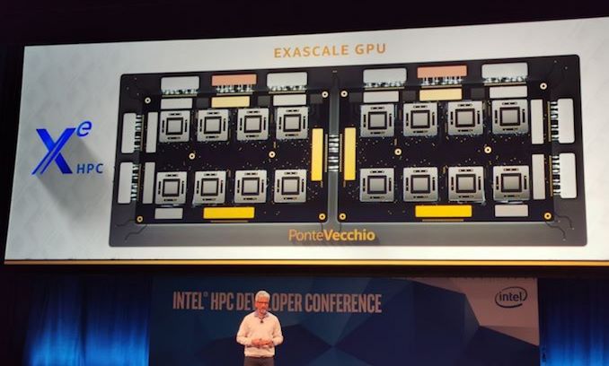
It has been a couple of weeks since Intel formally provided some high-level detail on its new discrete graphics strategy. The reason for the announcements and disclosures centered around Intel’s contract with the Department of Energy to build Aurora, an exascale supercomputer at the Argonne National Laboratory. The DoE and Argonne want developers clued into the hardware early, so when the supercomputer is deployed it can be used with as little ‘learning time’ as possible. This means Intel had to flesh out some of its strategy, as well as lift the lid on its first announced discrete GPU product. Only time will tell if it’s a bridge too far, or over troubled water, but today we know it as Ponte Vecchio.
Intel On Discrete Graphics: A Quick Recap
While Intel has had a graphics portfolio for a couple of decades, those graphics solutions have been limited to embedded graphics and integrated graphics solutions. There was a slight attempt to move into the graphics space and play with the big boys, with the Intel i740, however that was a long time ago. Intel’s current graphics architecture, called ‘Gen’, is currently in use in hundreds of millions of mobile devices, and is present in a substantial number of desktop processors, even if a discrete GPU is being used instead.
Intel has had high hopes for the graphics space before. Known as ‘Larrabee’, Intel attempted to engineer what was essentially x86 based graphics: using wide vector engines based on the same code path as Intel CPUs, the idea was to provide high-end graphics performance with the ease of programming in standard CPU code. While that product did actually run a number of graphics demos over the years, the hardware ended up being put to use in the high-performance computing market, where some developers saw the use of five-dozen 512-bit wide vector units absolutely fantastic for their simulations. This was the birth of AVX-512, which has lived on and now in Intel’s Xeon Scalable CPUs as well as consumer-grade Ice Lake laptop processors. The product that ‘Larrabee’ ended up as, Xeon Phi, scored a number of supercomputer wins and originally the Xeon Phi ‘Knights Hill’ product was destined to be put into Aurora in 2020. However the Xeon Phi program only lasted a few generations, with the final ‘Knights Mill’ hardware not being widely deployed and subsequently put to pasture.
Fast forward several years, and some management adjustments, and Intel has decided once again to enter the big graphics market. This time they’re going with something more conventional, something that looks more like a traditional graphics design. While the project started somewhere around three years ago, the big announcement that Intel was serious was when the company hired Raja Koduri, AMD’s Chief Graphics Architect in December 2017, and then Jim Keller, renowned SoC Guru. Raja Koduri’s title, Chief Architect, and his two decade of experience in building graphics solutions at AMD and Apple showcased how serious Intel was with this.
Since December 2017, Intel hasn’t said much about its new graphics plans. Under Ari Rauch, notable marketing figures and analysts were hired to be part of the team. Intel disclosed at its Architecture Day in December 2018 that the graphics solutions it would offer would be a full top-to-bottom implementation, covering low power integrated graphics all the way to the high-end. At the time Intel stated there would be two main GPU microarchitectures, all building from the ‘Xe’ architecture. Xe is meant to stand for ‘eXascale for Everyone’ (rather than x^2.718), with the marketing message that Intel wants to put high-end performance and efficiency anywhere it can.
As part of HPC DevCon, and Intel’s announcement with the DoE/Argonne, the veil was lifted, and we were told very slightly more than just the high level information. We were lucky enough to speak with Raja Koduri in a worldwide exclusive for the event, as his first official 1-on-1 interview since he joined Intel. It is worth a read and gives his perspective on a lot of ideas, as well as some of the decisions he has made.

This article is going to dive into Intel’s HPC DevCon disclosures about their graphics strategy. Here we are going to cover some of the blurb about Intel’s big plans, the new ‘third’ microarchitecture in Xe called Xe-HPC, the new GPU product ‘Ponte Vecchio’, Intel’s new Memory Fabric, a breakdown of the oneAPI software stack as presented, and what all this means for the rest of Intel’s graphics platform.
Exascale for Everyone
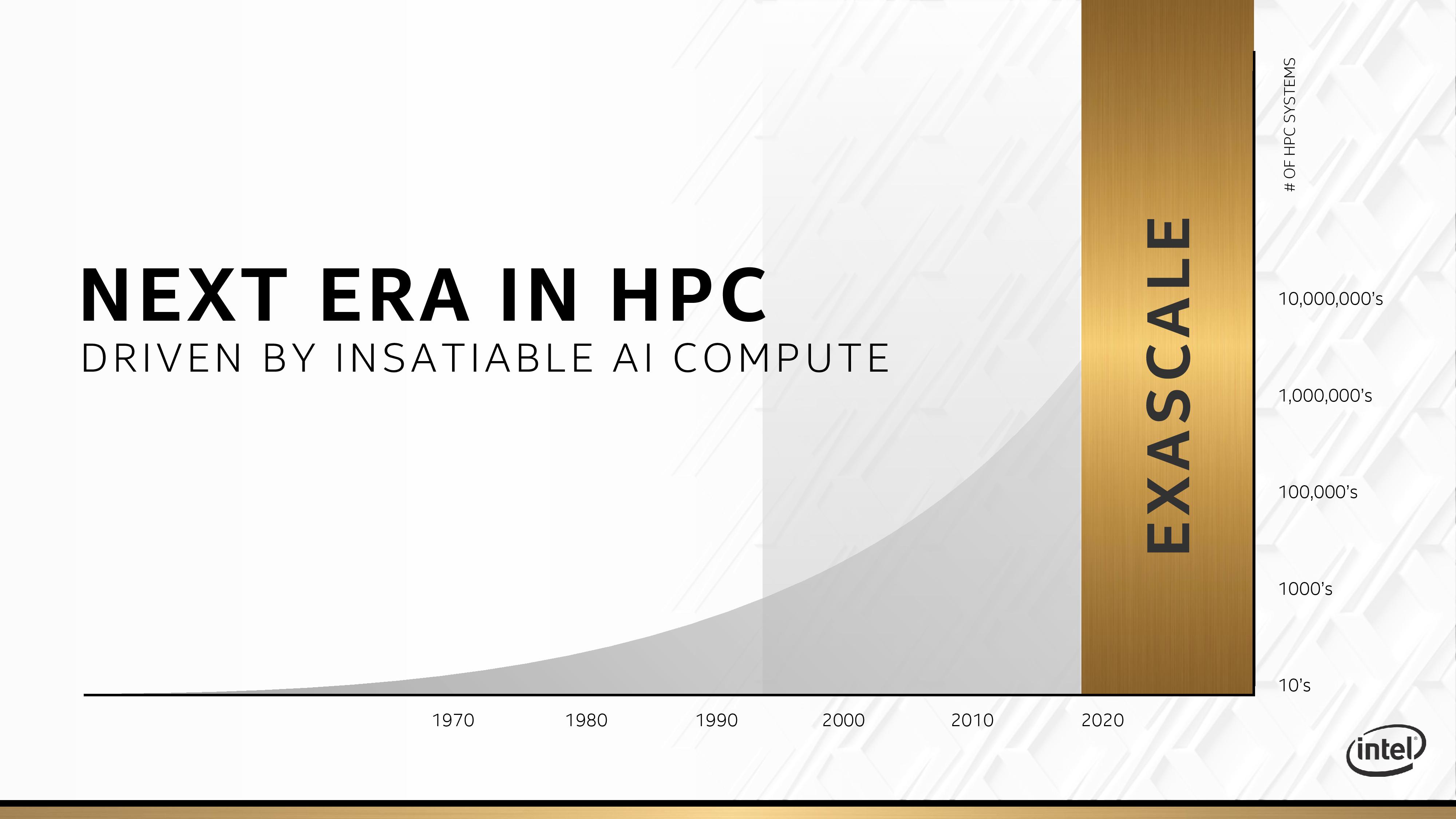
Intel says that it is hard not to notice the ‘insatiable’ demand for faster, more power efficient compute. Not only that, but certain people want that compute at scale, specifically at ‘exascale’. (It was disclosed at a high-performance supercomputing event, after all). For 2020 and beyond, Intel has designated this the ‘Exascale’ era in computing, where no amount of compute is good enough for leading edge research.
On top of this, Intel points to the number of connected devices in the market. A few years ago analysts were predicting 50 B IoT devices by 2020-2023, and in this presentation Intel is saying that by mid-2020 and beyond, there will be 100 billion devices that require some form of intelligent compute. The move to implementing AI, both in terms of training and inference, means that performance and computational ability have to be ubiquitous: beyond the network, beyond the mobile device, beyond the cloud. This is Intel’s vision of where the market is going to go.

Intel splits this up into four specific categories of compute: Scalar, Vector, Matrix, and Spatial. This is certainly one blub part of the presentation I can say I agree with, having done high-performance programming in a previous career. Scalar compute, is the standard day-to-day compute that most systems run on. Vector compute is moving to parallel instructions, while Matrix compute is the talking point of the moment, with things like tensor cores and AI chips all working to optimize matrix throughput. The other part of the equation is spatial compute, which is derived from the FPGA market: for sparse compute that is complex and can be optimized with its own non-standard compute engine, then an FPGA solves it. Obviously Intel’s goal here is to cover each of these four corners with dedicated hardware: CPU for Scalar, GPU for Vector, AI for Matrix, and FPGA for Spatial.

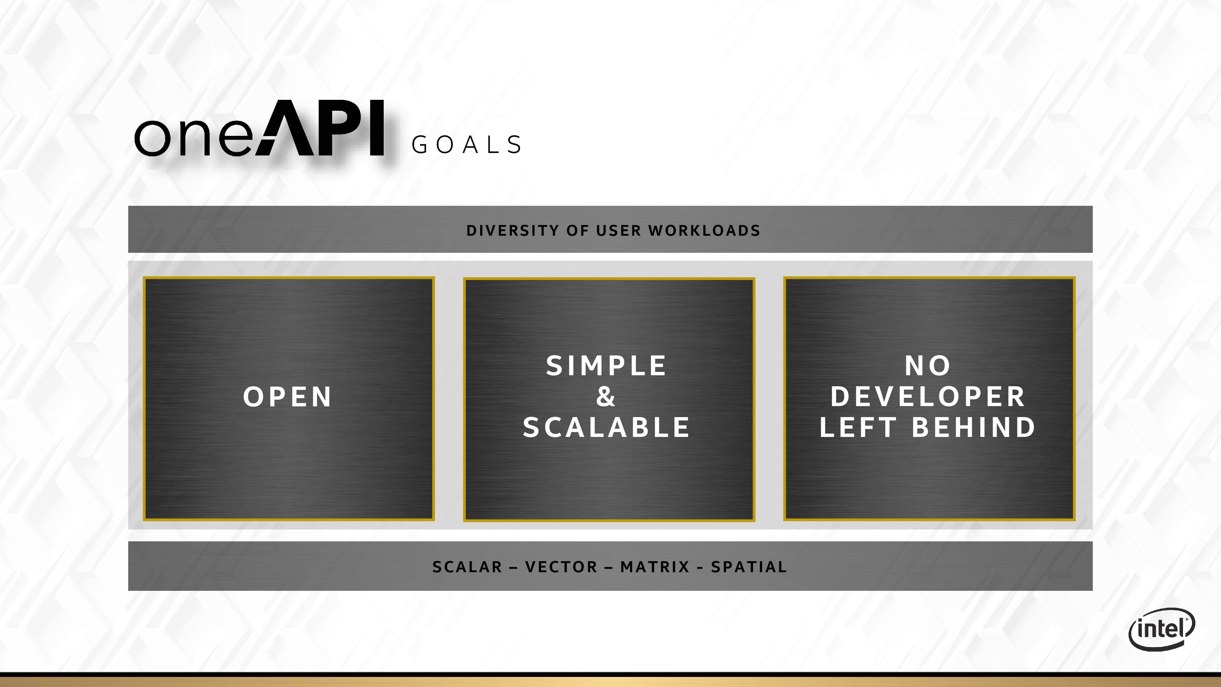
One of the issues with hardware, as you move from CPU to FPGA, is that it becomes more and more specialized. A CPU for example can do Scalar, Vector, Matrix, and Spatial, in a pinch. It’s not going to be much good at some of those, and the power efficiency might be poor, but it can at least do them, as a launching point onto other things. With GPU, AI, and FPGA, these hardware specializations come with different amounts of complexity and a higher barrier to entry, but for those that can harness the hardware, large speed-ups are possible. In an effort to make compute more ubiquitous, Intel is pushing its oneAPI plan with a singular focal resource for all four types of hardware. More on this later.
Intel’s Xe architecture will be the underpinning for all of its GPU hardware. It represents a new fundamental redesign from its current graphics architecture, called ‘Gen’, and pulls in what the company has learned from products such as Larrabee/Xeon Phi, Atom, Core, Gen, and even Itanium (!). Intel officially disclosed that it has its first Xe silicon back from the fabs, and has performed power cycling and basic functionality testing with it, keen to promote that it is an actual thing.
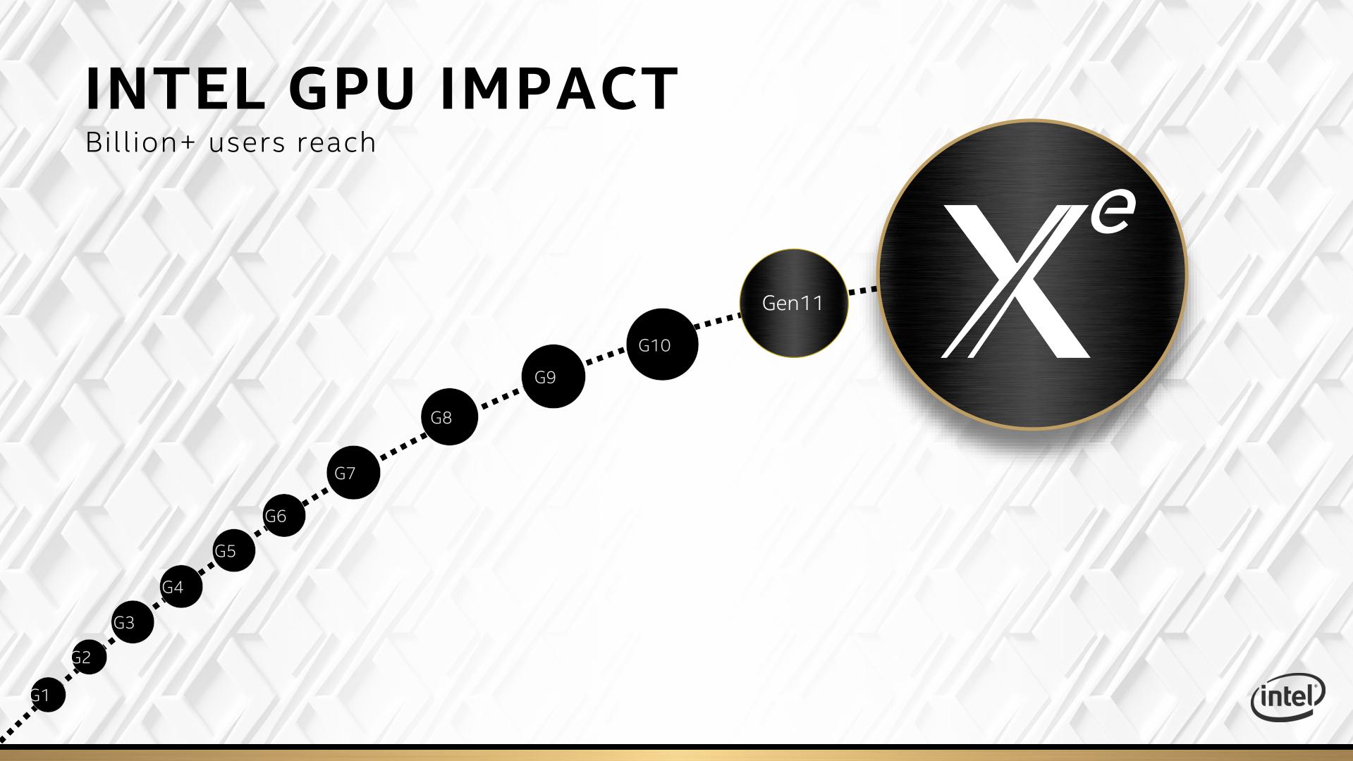
So far the latest ‘Gen’ graphics we have seen is the Gen11 graphics solution, which is on the newest Ice Lake consumer notebook processors. These are out in the market, ready to buy today, and feature performance 2x over the previous Gen9/Gen9.5 designs. (I should point out that Gen10 shipped in Cannon Lake but was disabled: this is the only graph ever where I’ve seen Intel officially acknowledge the existence of Gen10 graphics.) We have seen diagrams, either potentially from Intel or elsewhere, showing ‘Gen12’. It would appear that ‘Gen12’ was just a holding name for Xe, and doesn’t actually exist as an iteration of Gen. When we asked Raja Koduri about the future of Gen, he said that all the Gen developers are now working on Xe. There are still graphics updates to Gen, but the software developers that can be transferred to Xe have been already.
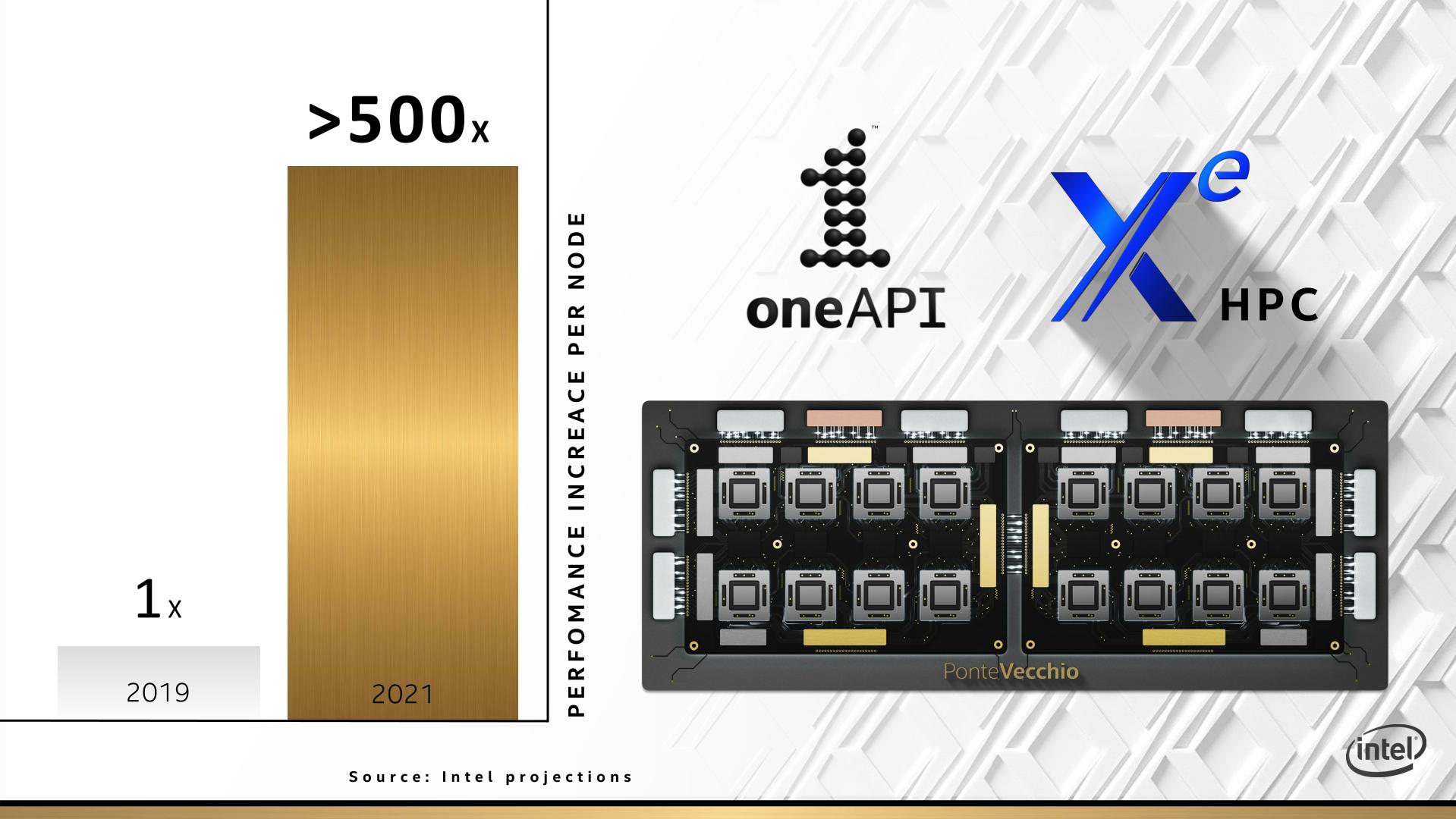
If you’re only going to read one thing today, then I want to skip ahead to Raja’s final slide of what he presented at HPC DevCon. Putting a quite ambitious goal in front of the audience, it showed that Intel wants to be able to provide a 500x in performance per server node by the end of 2021 compared to the per-node performance in 2019.
Now it is worth noting that this goal wasn’t specifically nailed down: are we comparing vector code running in scalar mode on a single 6-core Xeon Bronze in 2019 to an optimized dual-socket with six Xe GPUs in 2021? 500x is a big bet to make, so I hope Intel is ready.
In the next few pages, we’ll cover Xe, Ponte Vecchio, oneAPI, and Aurora.
Xe: Flavors and Architecture
Unlike Baskin Robbins, only 3 Flavors
Prior to the disclosures made at HPC DevCon, Intel had previously stated that its Xe design, the Xe architecture, would stretch from integrated graphics all the way through to mid-range graphics, enterprise graphics, and then into the datacentre for use in AI, acceleration, virtualized graphics, and everything else. At the entry level, users should expect ‘TeraFLOPs’ of performance, while at the datacenter level there will be ‘PetaFLOPs’ of performance. The graph looked something like this:
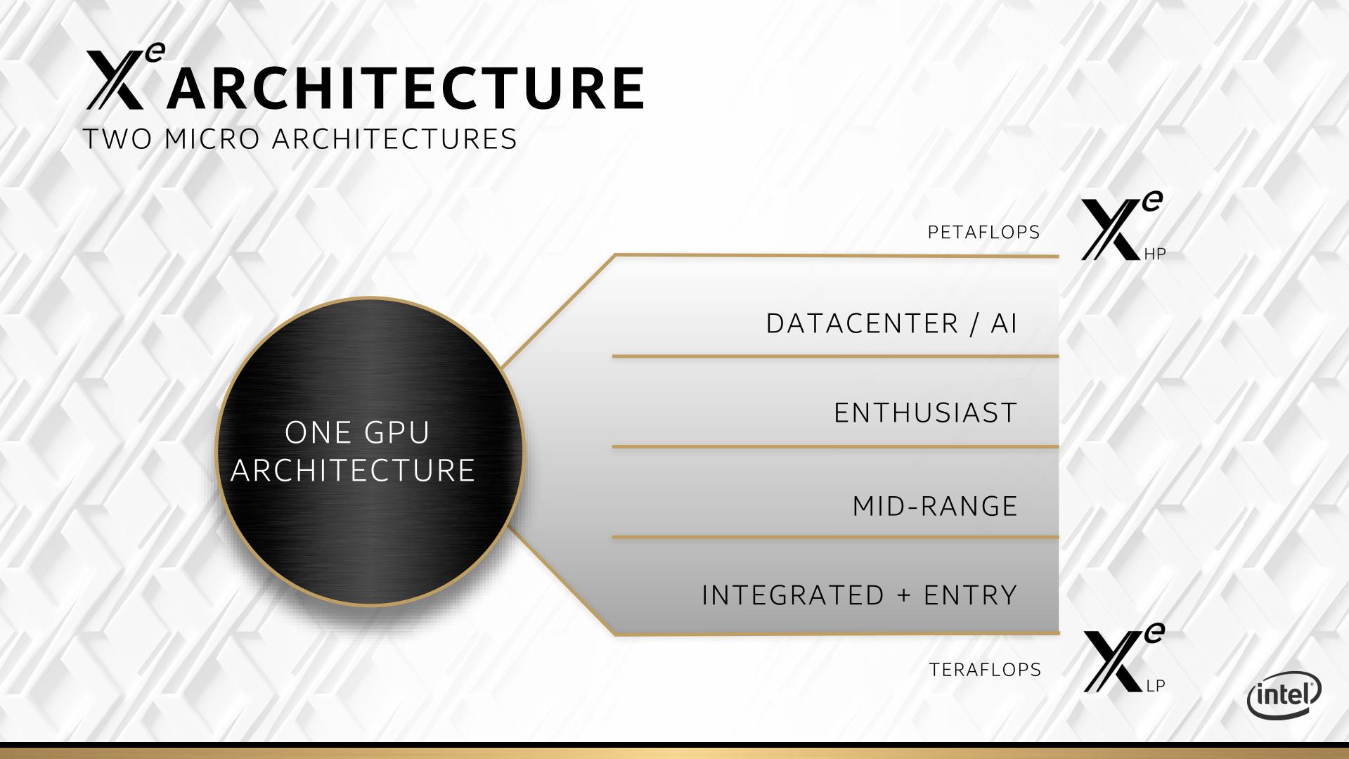
At the time Intel specified that there would be two versions of Xe across this whole range. One of the big reveals of Intel’s announcements was not only the emergence of a third variant of Xe, but also the naming of all three variants.
At the entry level will be Xe-LP, or Low Power. This will cover all of the integrated graphics solutions – Raja Koduri said that that the design of LP would push up to 20 W of graphics power. He also stated that the LP design is scalable, up to 50 W, but there are no plans to launch LP at that power as it becomes less power efficient. By this, we should expect to see LP in traditional mobile form factors up to 45 W, and probably in monolithic desktop CPUs. From this, we should surmise that LP is strictly for mobile and integrated graphics solutions, and unlikely to be available in a discrete form. By discrete, I mean a PCIe card form factor – if Intel were to make discrete LP silicon as products, it might be available to extend what is already available in notebook form factor processors.
For the mid-range, enthusiast, and datacenter, we have Xe-HP, or High Power. This is where Intel’s discrete form factor graphics is going to play, likely everything from 50 W up to 250 W or higher. Given the importance of the discrete graphics card space, Intel is going to have to attack with Xe-HP with both hardware and software support, including day-0 drivers. Intel didn’t go into any detail regarding Xe-HP, which we expect to be presented sometime in 2020.
The new third arm will be Xe-HPC, or High Performance Computing. Where the LP and HP variants will have an angle of graphics output to them, HPC is all about improving raw throughput.

The new Ponte Vecchio GPU, which we’ll talk about in the following pages, falls under this Xe-HPC microarchitecture. Intel was clear to point out that Xe-HPC isn’t so much ‘a new high level’ version of Xe, but moreso that it will cover the compute heavy workloads compared to the graphics heavy workloads. A great diagram they put out was this:
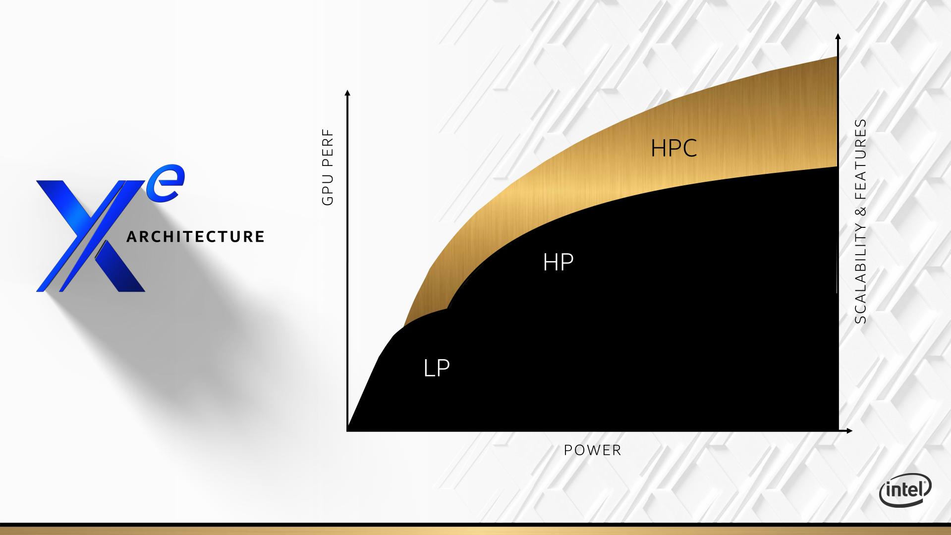
This shows LP taking the low end market, HP going for a higher performance overtone, and then HPC will scale all the way from the top of LP, through all of HP, and beyond HP. Because the supercomputer deployments that use this hardware can better accommodate higher power consumption hardware than normal high-end PCs or even servers, the HPC variants are likely to go up to 400W or even more (we saw a PCIe card with a 500W TDP this year at Supercomputing, so that might be a new norm).
Structurally Sound: Architecture
Every GPU design is fundamentally built upon its vector width capability. A GPU is a big fancy vector machine, and so a balance has to be made between super wide vectors that can accommodate lots of calculations against lots of tiny vector machines that can do things in parallel. One of the biggest drivers for vector width comes back to graphics calculations: being able to manipulate a certain number of pixels within a vector with at the right time, and dealing with data coming from different places in memory, or perhaps even dealing with different kernels working on different sets of data.
Vector width also defines a lot of the software and a lot of optimizations. When speaking to Raja Koduri as part of the disclosures, he stated that trying to translate code built for a large vector width down to a smaller vector width was actually quite difficult. To that end, Xe is built with a variable vector width.
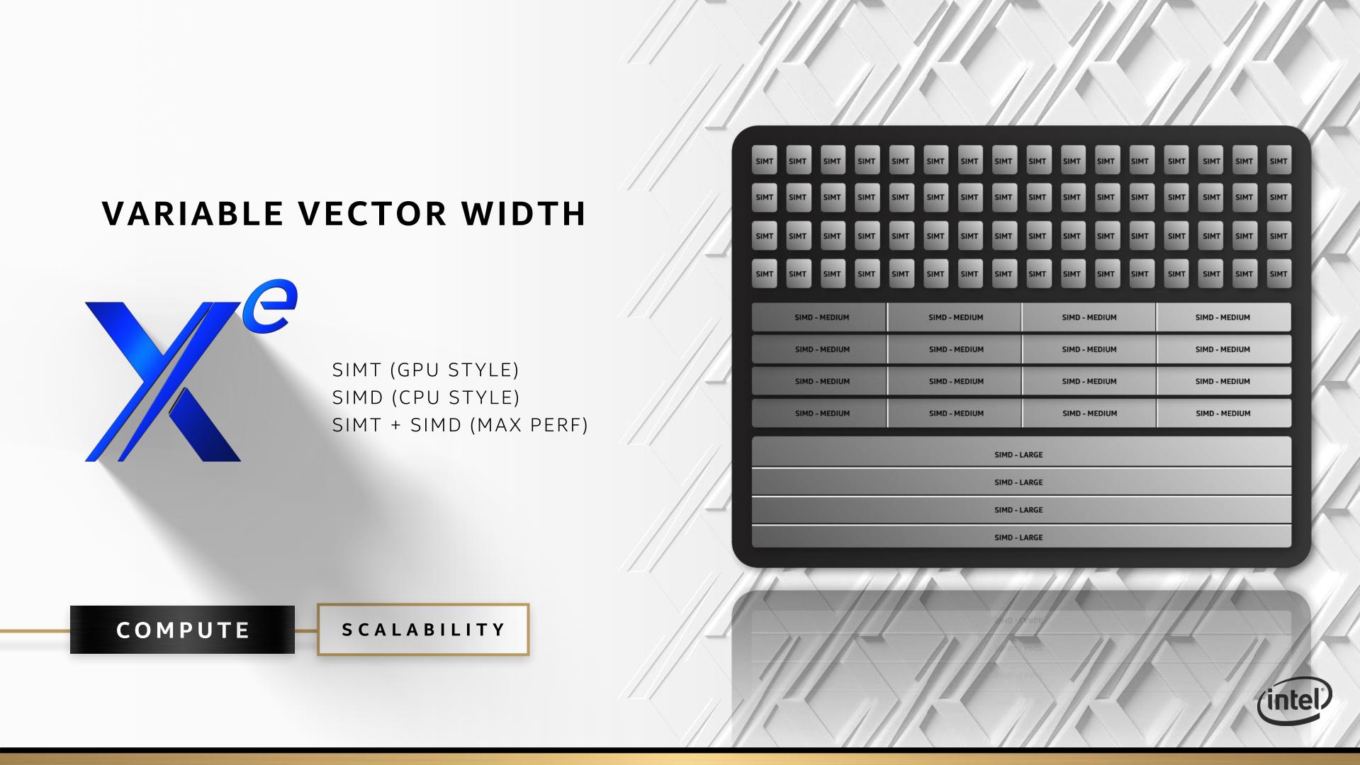
Xe contains two fundamental units: SIMT and SIMD. In essence, SIMD (single instruction, multiple data) is CPU like and can be performed on single elements with multiple data sources, while SIMT (single instruction, multiple threads) involves using the same instructions on blocks of data, as part of the whole ‘vector’ processing thing. An Xe design can be built with a number of SIMT and SIMD modules in the correct order to deal with the precise nature of the workload for that market segment. Welcome to GPU building, Lego style.
Along with SIMT and SIMD, Intel stated that both parts can work together for ‘maximum performance’ mode. This almost sounds like stretching a potential SIMT command over the SIMD units, if that is even possible. But Intel stated that the design of each unit is meant to be scalable (because of exascale). In this instance, Intel was quite keen to promote that its Xe architecture, with SIMT and SIMD units in its Xe-HPC designs at least, can scale to 1000s of units.
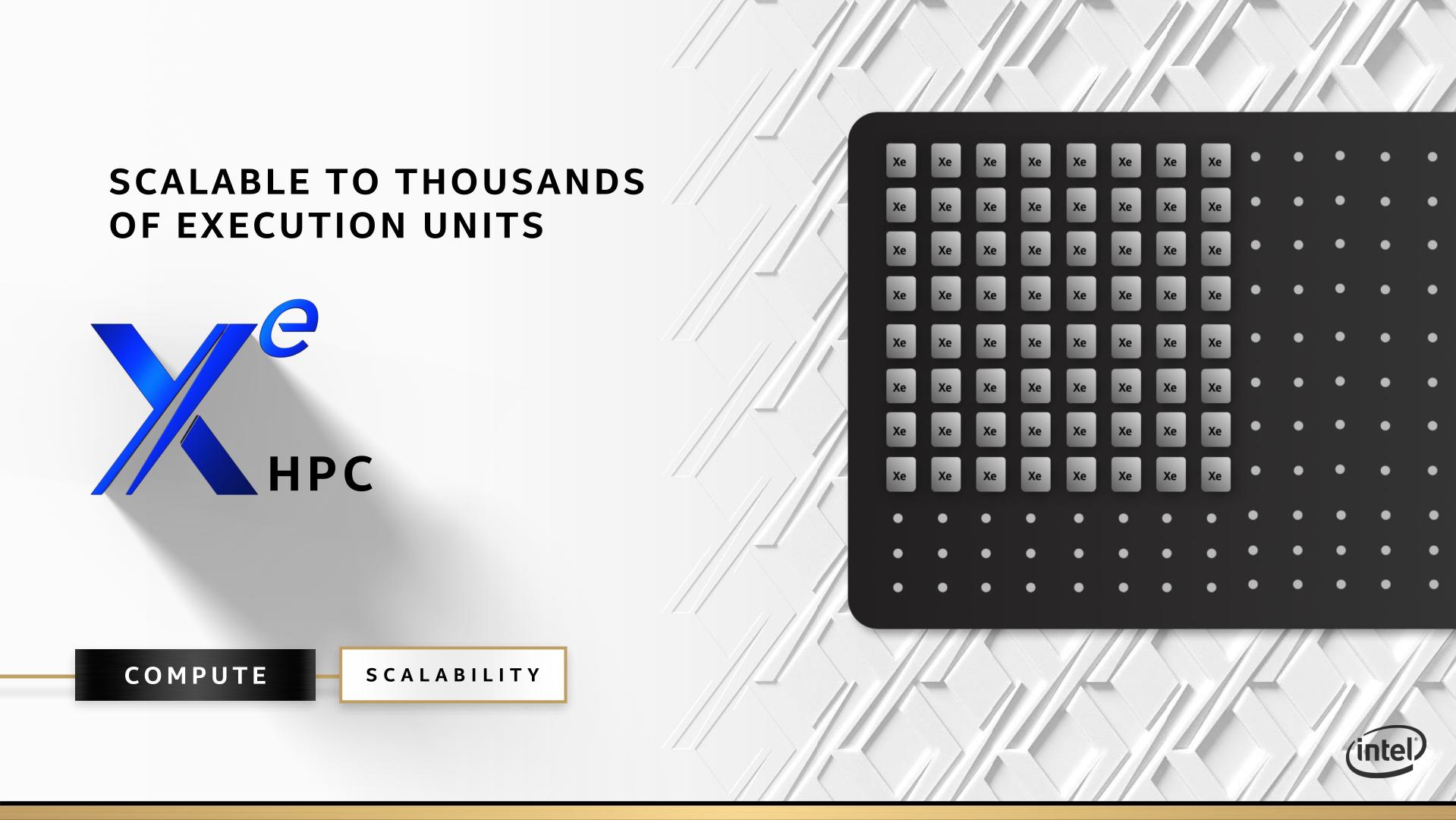
In that diagram it shows an 8x8 grid, with dots spreading to a 14x11 grid, but I don’t think there’s anything we can infer from this diagram.
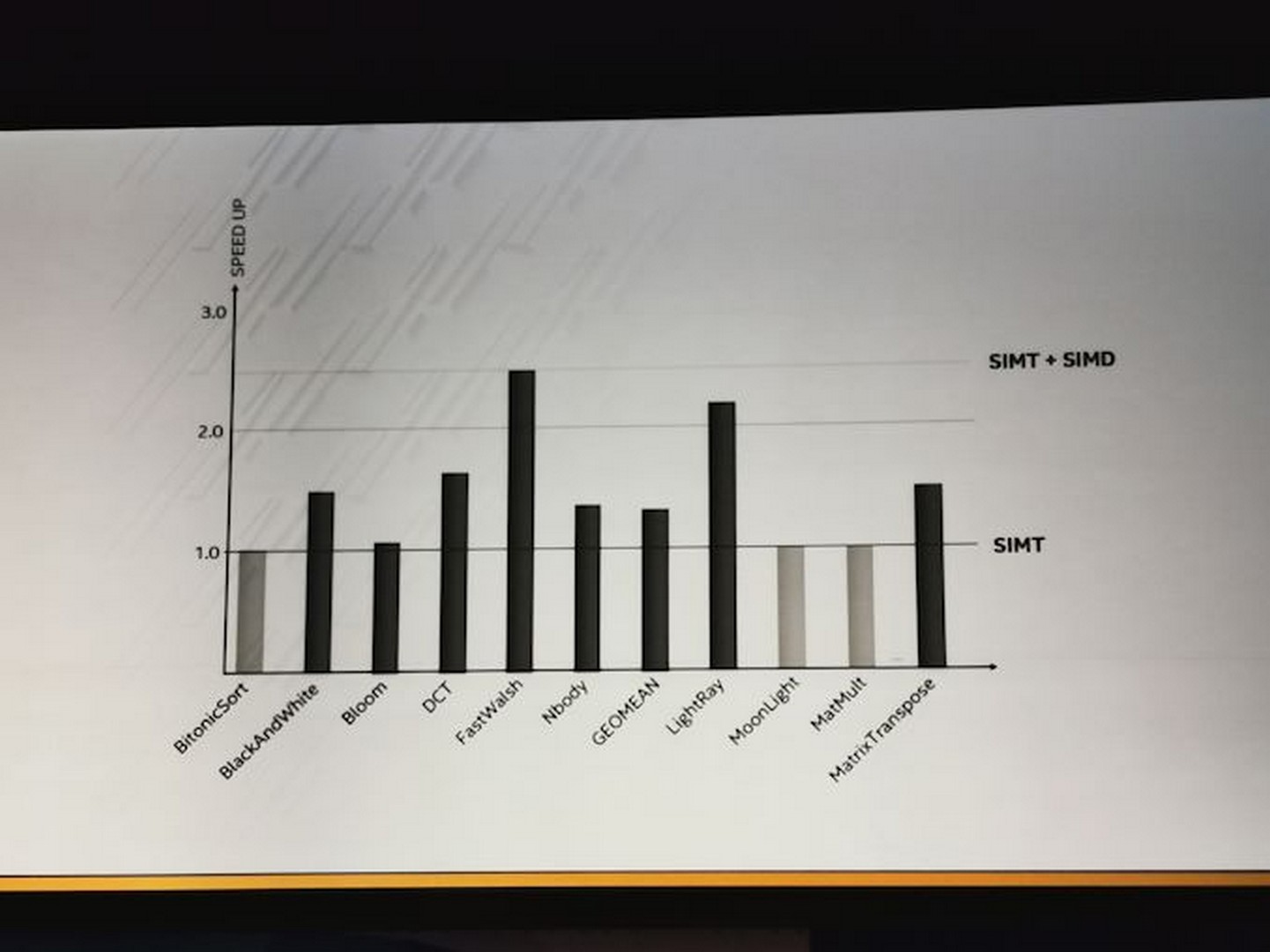
Based on Intel’s in-house simulations, they showed some areas where the combined SIMD+SIMT would help. In this instance, some of the standard SIMT codes don’t experience any speed-up and can only use SIMT units: a bitonic sort, the MoonLight ray tracer, and Matrix Multiply (that’s a big one). Other codes can experience speed-up with SIMT+SIMD combined, such as Matrix Transposing, N-body simulations, the LightRay ray tracing engine, and the biggest uplift is in FastWalsh.
What this graph suggests is that for code that is fully optimized for SIMT, then no extra SIMD is needed and they will remain idle. For code that relies on some serial work, such as N-body, or for ray tracers that are programmed differently, then when a kernel needs to perform some serial work it can move those threads to SIMD/CPU part of the hardware and proceed that way rather than having to go back to the CPU. This can be important for a lot of code speedups, but for those that are already heavily optimized for vector compute, then the presence of the SIMD units just mean wasted silicon space – keep note of that.
Execution Unit Design: A High Level
Intel was kind enough to showcase what goes into one of these Xe units, but only in the sense of a block diagram with not a lot of information.

I should state that this slide is an Xe-HPC unit, which means that other LP/HP units might look similar but have different weighting of features. It doesn’t state if this is a SIMT or SIMD unit, but this is likely a SIMT unit given what we can deduce.
If this diagram looks relatively familiar, then I share those thoughts. It looks to be an upgraded diagram of one of the execution units from Intel’s Gen graphics architecture. For a quick re-cap, that architecture was based on a 7-way pipeline with 7 threads per EU. In this instance, it is very easy to see that an Xe-HPC unit has an 8-way outline, which likely indicates 8 threads in parallel if the diagram is an accurate representation.
There’s no way to tell what sort of operations each thread can do, but the blocks on the left are likely to be for different thread functions, such as a pair of special function units at the top, while the two groups of four might be for AES instructions, or memory load/store ports, or local caches.
All we really know for sure is that Intel is putting a lot of effort in this Xe-HPC unit to support double precision. This is important, and to explain why we need to cover some truths about the high-performance computing landscape.
At the advent of GPU programming, with the wonderful delights of the early versions of CUDA, the focus was on single precision throughput: known as 32-bit floating point, or FP32. For anyone doing scientific simulations, depending on the type of work you were doing, this was either great and super-fast, or it very quickly reached a point where single precision was not enough.
I was lucky enough during my PhD to cover topics that landed on both sides of the fence, but what annoyed me was when FP32 wasn’t enough: my simulations were producing results as expected, and then suddenly flat-lined when the changes that were meant to be happening in the simulation happened to such a fine degree that FP32 didn’t have enough significant figures to compensate.
As a result, I had to switch most of my compute and data types to double precision, or FP64. This gave me another dozen or so significant figures per value, but it also put all sorts of stresses on my workloads in terms of register pressure, cache pressure, and the design had to be changed in parts to accommodate. In order to get to the same point in the simulation with FP32 and FP64 meant FP64 took longer, but I could go further and actually have meaningful results.
Thankfully at that time, NVIDIA was fairly reasonable with FP32/FP64 balancing. If it wasn’t a strict 1:1 then at least a 1/2 rate or 1/3 rate was quite sufficient, especially when it was needed. When the 1/32 rate hardware came along, we all thought it was a ploy to encourage low cost academic simulator students onto the high cost stuff, not that it was because the cards dedicated more silicon to graphics-heavy workloads.
For a long time, FP64 compute has reigned supreme. Then this thing called AI came along, with its high compute requirements for training. AI compute requirements are certainly driving the industry forward, however there seems to be arguments about performance and throughput: depending on which researcher you talk to, each might have a different preference to how precise the numbers need to be. There is a trade-off between training accuracy, training time, and compute throughput when we discuss low precision numbers (INT8, FP16) with high-precision numbers (FP32, FP64). Between training and inference (Facebook needs a lot of inference, for example) there has been a big push towards low precision compute.
So here we have two sides of the coin: FP64 for the simulators, those that deal with oil/gas, astronomy, geology, weather dynamics, and some financial analysis, while AI training works mostly in FP16/BF16 and AI inference likes INT8/FP16.
Intel’s play here with Xe-HPC is for the FP64 crowd. The promise with Xe-HPC is a 40x increase in FP64 compute performance. That being said, they didn’t say compared to what – to an old Gen design?
At this point, this is all we know about how Xe Execution Units might look, and most of the detail here applies to Xe-HPC only. What functions / balancing will go for LP or HP is unknown at this point, but I’d hazard a guess and say that those designs are built more like shader cores for graphics purposes.
XeMF: The Scalable Memory Fabric, with RAMBO CACHE
While Intel was keen to point out that the Xe-HPC execution units can scale to 1000s of units, scaling means nothing without the right way to move data in and out of those compute engines. To that end, Intel disclosed that it has developed a memory fabric for its Xe-HPC designs called XeMF.
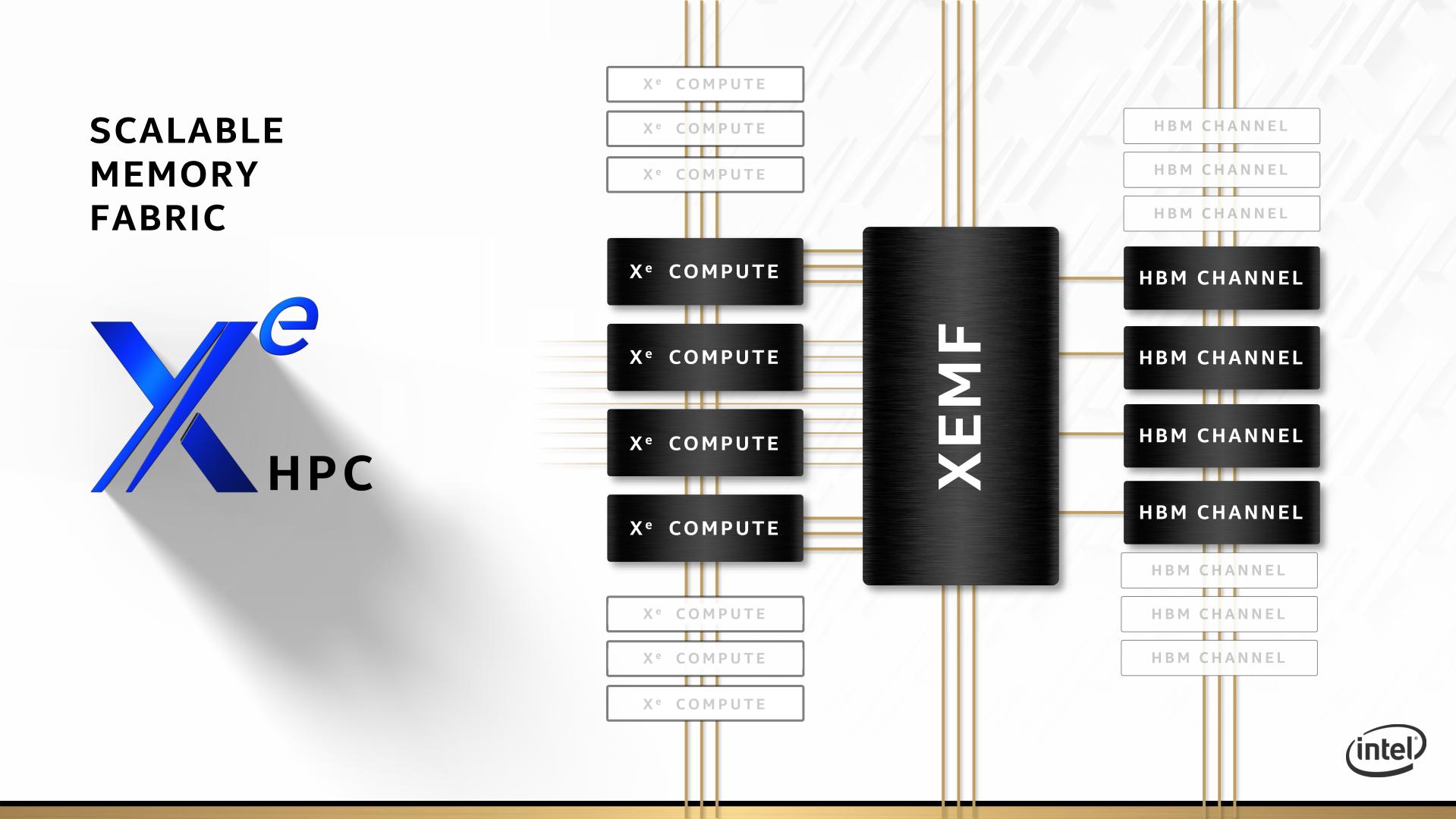
The scalable memory fabric sits between the compute units and any attached memory – in this diagram in this instance we see HBM listed. Assuming this diagram is accurate, there are few takeaways we can get from this.
Firstly, the XeMF has three connections to each Xe-HPC compute unit (XeCU), while it only has one connection to each HBM channel. That’s a 3:1 factor in bandwidth, which might be a limitation of off-silicon data transfer.
Also, each XeCU seems to have direct connections with each other without needing to use the fabric. Again, it shows 3 connections between each XeCU, and it shows that an XeCU can only communicate with its two nearest neighbors. The diagram is showing the XeCUs in a linear fashion, which might just be for the simplicity of the diagram.
The diagram also shows each HBM channel able to speak to the next door HBM channels without going through the fabric. If that’s true, that’s new.
Then there are the connections at the top of the bottom of the fabric, likely extending the fabric to more chips. We’ll see about that in a second.
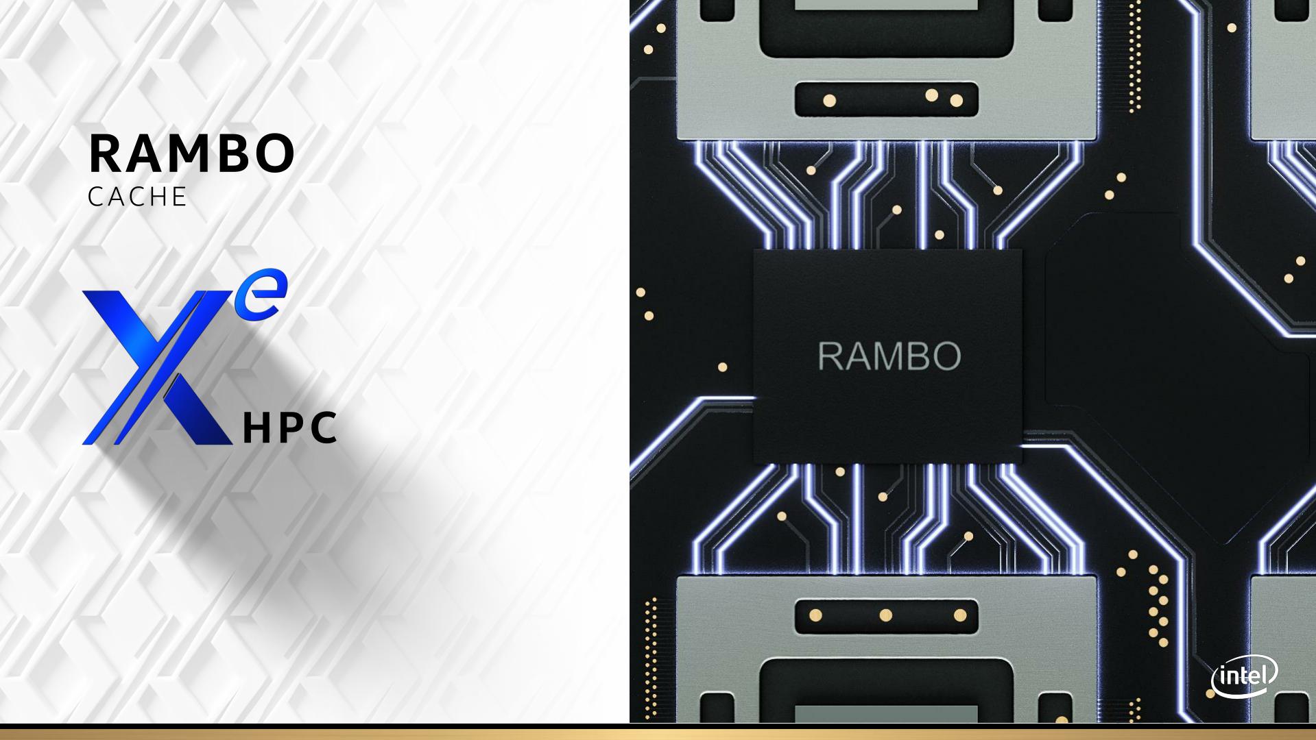
Even though I missed the picture, the next slide in this deck shows that the XeMF has a secret surprise: a special cache. In this instance it has been dubbed a ‘RAMBO’ cache, although after speaking with Raja, this won’t be the actual marketing name for this feature. What the RAMBO cache does is offer a large amount of cache for the XeCUs to call upon and store data for future use. Given that the lines on the diagram show that the cache to CU bandwidth has a 3:1 improvement over cache to HBM, then storing data for future compute is likely what this is for, as it can supply it to the CUs at a much higher bandwidth. The slide implies that the RAMBO cache is inside the XeMF chips, but in another side it says that Foveros is used in the RAMBO cache, so it might actually be distributed through the whole GPU design.
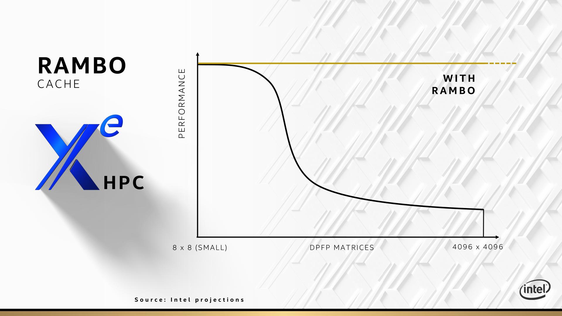
In the next slide, this is exactly what Intel tells us. Here Intel is giving the example of FP64 matrices, but doesn’t specify if this means compute or streaming bandwidth. In this instance without the RAMBO cache, the XeCU would be at peak performance with an 8x8 matrix, probably start declining somewhere around the 64x64 or 256x256 matrix, down to a low point at a 4096x4096 matrix. With the RAMBO cache, according to Intel, the ‘performance’ (again, not sure if compute or streaming), will be the same on 4096x4096 matrices as 8x8 matrices. For a lot of simulation work, that’s going to be a great addition.
A final word about the fabric: there’s no telling if XeMF will come to LP or HP designs – Intel only spoke about XeMF in the context of HPC.
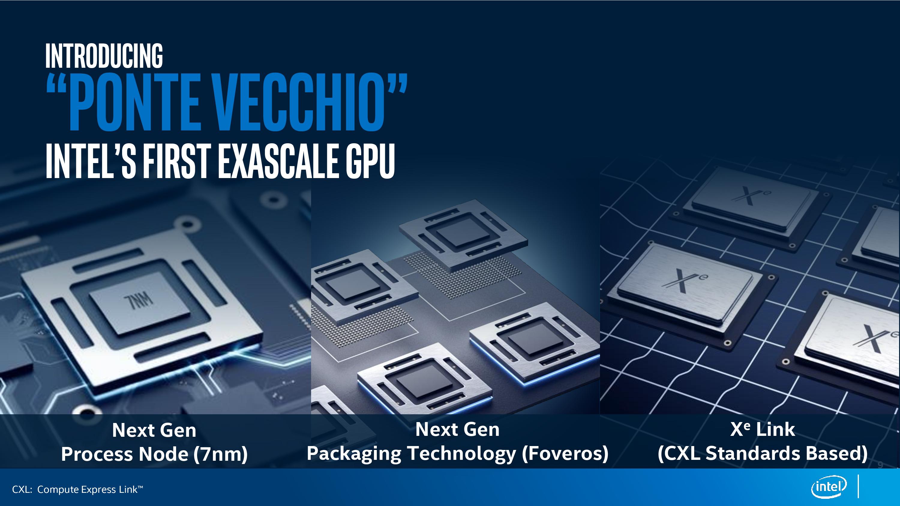
Ponte Vecchio: The Old Bridge in the land of Gelato
With the disclosures about Xe-HPC and the new compute unit and memory fabric in mind, Intel went onto the big money announcement: the first Xe-HPC GPU will be a design called Ponte Vecchio (PVC).
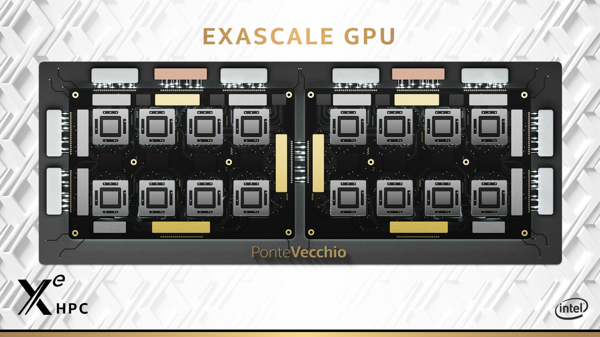
If that looks like a weird GPU to you, then I agree. What we have are two segments, each with eight compute chiplets, a number of XeMF chips, and HBM memory. I do want to step back a second to talk about some of the technologies around PVC before going into what we see here.
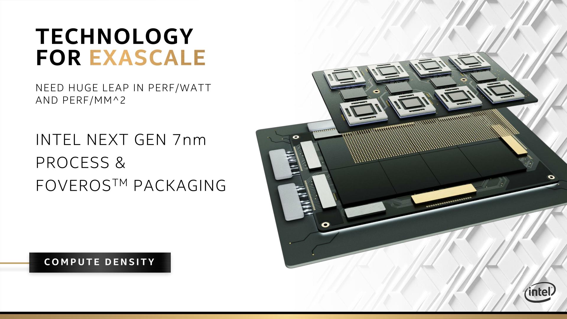
Earlier in 2019, I was offered a chance to speak to Intel’s Ramune Nagisetty. She’s in charge of Intel’s plans regarding chiplet and connectivity technologies: she’s the person to speak to when it comes to connecting chiplets with technologies like the Embedded Multi-Die Interconnect Bridge (EMIB), but also when it comes to new stacking technologies like Foveros. We’ve already seen EMIB in a number of products, such as Intel’s FPGA family, and consumer hardware like Kaby Lake-G, and Foveros is getting its first limelight in the new Lakefield chip for small-form factor client notebooks, which stacks a 14nm IO die with a 10nm Compute Die, all with a DRAM PoP on top.
In that discussion, it was confirmed what Raja had said at the Architecture Day a few months prior: both EMIB and Foveros will be coming to Intel’s new family of GPUs. Of course, EMIB and Foveros doesn’t come cheap: trying to align vias between silicon is best done when sober and with a clear head, and even then there are always optimizations to be made. In that regard, we assumed EMIB and Foveros would be going on the high-end discrete graphics solutions, what we now know to be Xe-HP. But it would appear that these technologies are likely to be in Xe-HPC as a priority, and Ponte Vecchio seems to be the first chip that will have both.
It is worth noting that technologies like EMIB and Foveros are going to define Intel’s future. Not only in GPUs, but also CPUs, FPGAs, AI, and everything else.
This slide shows that both technologies will be on Ponte Vecchio, but this slide actually says something a lot more than what it appears.
One of the questions with EMIB and Foveros is in what form it will take. There are many possibilities for both, and this slide might have exposed a few. Note that this slide only shows half of a Ponte Vecchio, and I want to do a custom diagram for you so show what I’m seeing here.
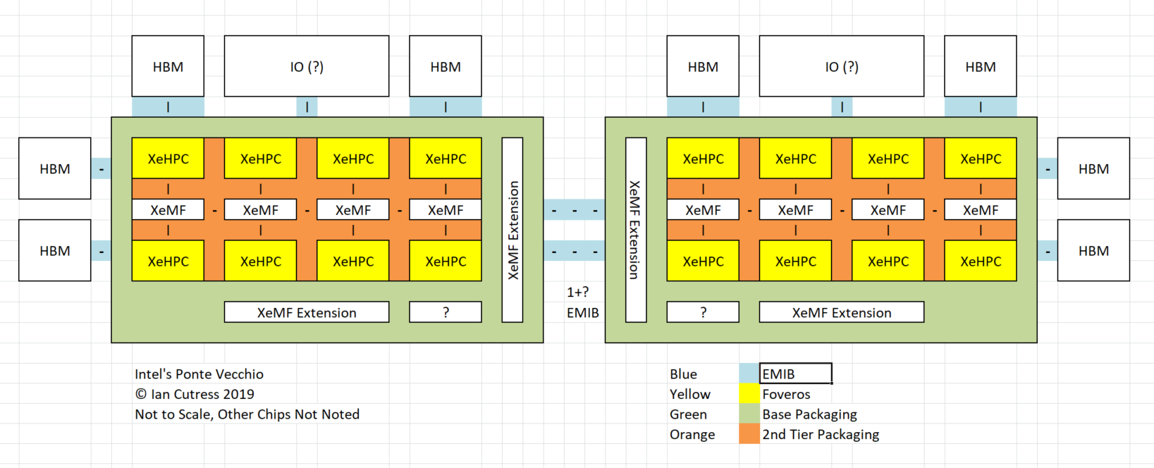
Here I’ve expanded out to a full PVC, with 16 Xe-HPC chiplets, 8 XeMF chips, and each half of the PVC has access to four HBM stacks. Each of the HBM stacks is connected via EMIB, along with what I think is an IO chip (perhaps built on 14nm).
From the official slide above, you will notice the group of 8 Xe-HPC chiplets and four XeMF chips seem to be on a separate package altogether, with a unified BGA onto another tier (the mid-tier) of packaging below. To be honest, that slide also looks like there are some chips on that mid package, but on this mid-package we also get the EMIB connections and what I believe is an XeMF scaling chip for off-GPU connections. The HBM2 and what IO chip seem to be on a bottom tier of packaging, which means that we have three tiers of packaging for this individual GPU: four if you include the Foveros on each of the Xe-HPC chiplets!
Now normally when we think of tiered packaging like this, we expect it to be BGA on BGA. There could be a part of this design that uses an interposer. If Intel was making this at TSMC, I might use the word ‘CoWoS’ as part of the stacking technology they use. At the minute it’s all a lot of guesswork. Assuming the diagram is accurate.
I’ve labelled each of the Xe-HPC chiplets as having Foveros, as we believe these to be two die stacked. A lot of commentary around this stacking is asking the question of what exactly are on each of the two dies that are stacked – is one IO and the other compute, like in Lakefield, or is it something else? A semi-reasonable conclusion is that one die might be cache, and the other die might be compute. However it’s important to note that GPUs tend to have local cache right next to the compute, to in actual fact I expect both of these dies in the Foveros stack to both be compute dies. It may be such that one is for SIMD and the other is for SIMT, but if the two were identical and modular then it makes it much easier to manufacture.
For those of you wondering what those metal brackets are around each of the Xe-HPC dies, those are likely to be shims to help correct for different chip heights. I should point out that the die inside the ship, the stacked Xe-HPC die, is actually smaller in the diagram than the XeMF die between each pair of chiplets. This could be for all the cache on the XeMF dies, or it could be if they are built on a different process node.
Also, it is worth noting that with Ponte Vecchio, we have two ‘slices’. From the diagram, it looks like that each slice has additional XeMF connection points, which could be used to go off-GPU, or so more slices (up to four) could be connected together. Some of that we might address when we look at the Aurora system and Intel’s proposed layout of one of the servers.
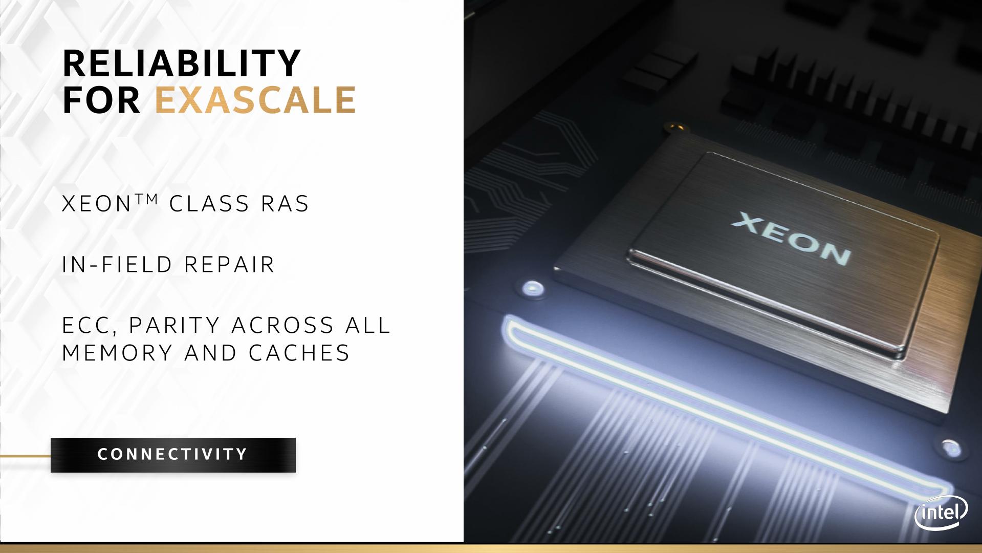
Intel promises a couple of other PVC features. Not only will the hardware support ECC and parity checks across all memory and caches, but there will be Xeon-class RAS features and something called ‘in-field repair’. More details to come.
Also, a final word on the name: Ponte Vecchio. Intel has plenty of Lakes, Coves, Rapids, and other things. Apparently having a codename that involves a physical place actually helps address any potential legal issues without having to do due diligence for a proper marketing name. Raja Koduri said that he chose it because it’s based in Florence, which has good gelato. He likes gelato, and should Intel decide to do a launch event with Ponte Vecchio in mind, Raja gets his gelato. I went to Florence a couple of years ago – the gelato was good.
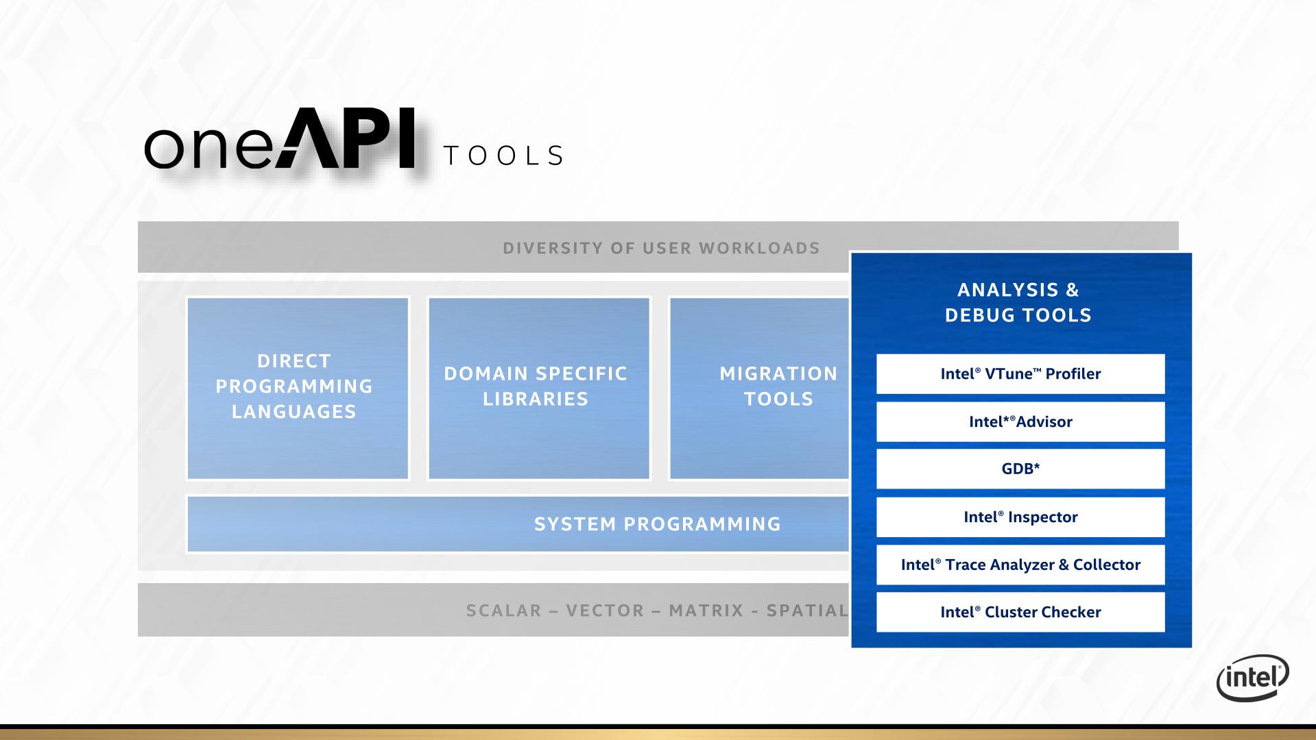
oneAPI: Intel’s Solution to Software
Having the hardware is all well and good, but the other angle (and perhaps more important angle) is software. Intel is keen to point out that before this new oneAPI initiative, it had over 200+ software angles and projects across the company to do with software development. oneAPI is meant to bring all of those angles and projects under one roof, and provide a single entry point for developers to access whether they are programming for CPU, GPU, AI, or FPGA.
The slogan ‘no transistor left behind’ is going to be an important part of Intel’s ethos here. It’s a nice slogan, even if it does come across as if it is a bit of a gimmick. It should also be noted that this slogan is missing a key word: ‘no Intel transistor left behind’. oneAPI won’t help you as much with non-Intel hardware.
This sounds somewhat too good to be true. There is no way that a single entry point can do all things to all developers, and Intel knows this. The point of oneAPI is more about unifying the software stack such that high-level programmers can do what they do regardless of hardware, and low level programmers that want to target specific hardware and do micro-optimizations at the lowest level can do that too.
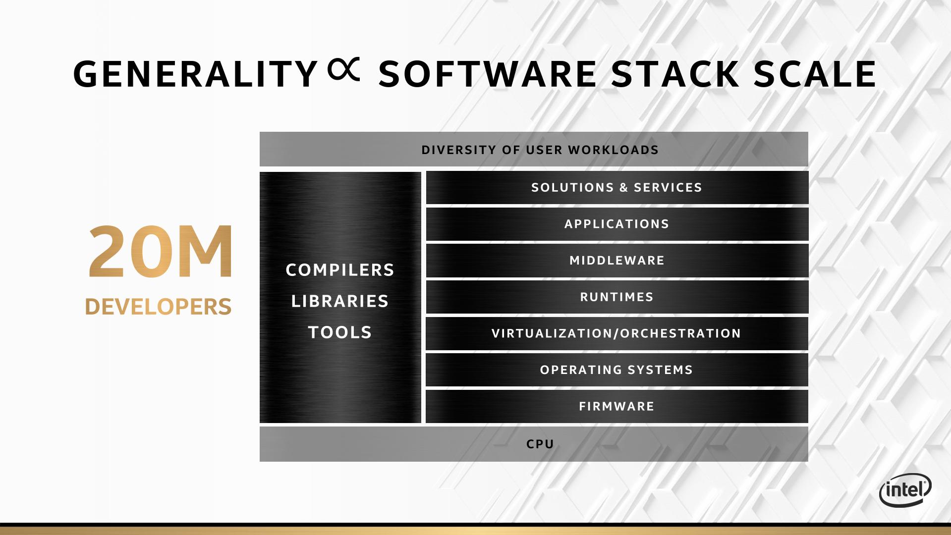
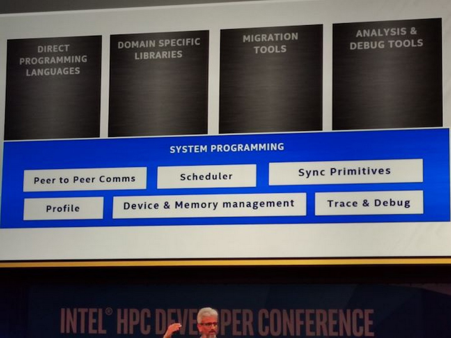
Everything for oneAPI is going to be driven through the oneAPI stack. At the bottom of the stack is the hardware, and at the top of the stack is the user workload – in between there are five areas which Intel is going address.
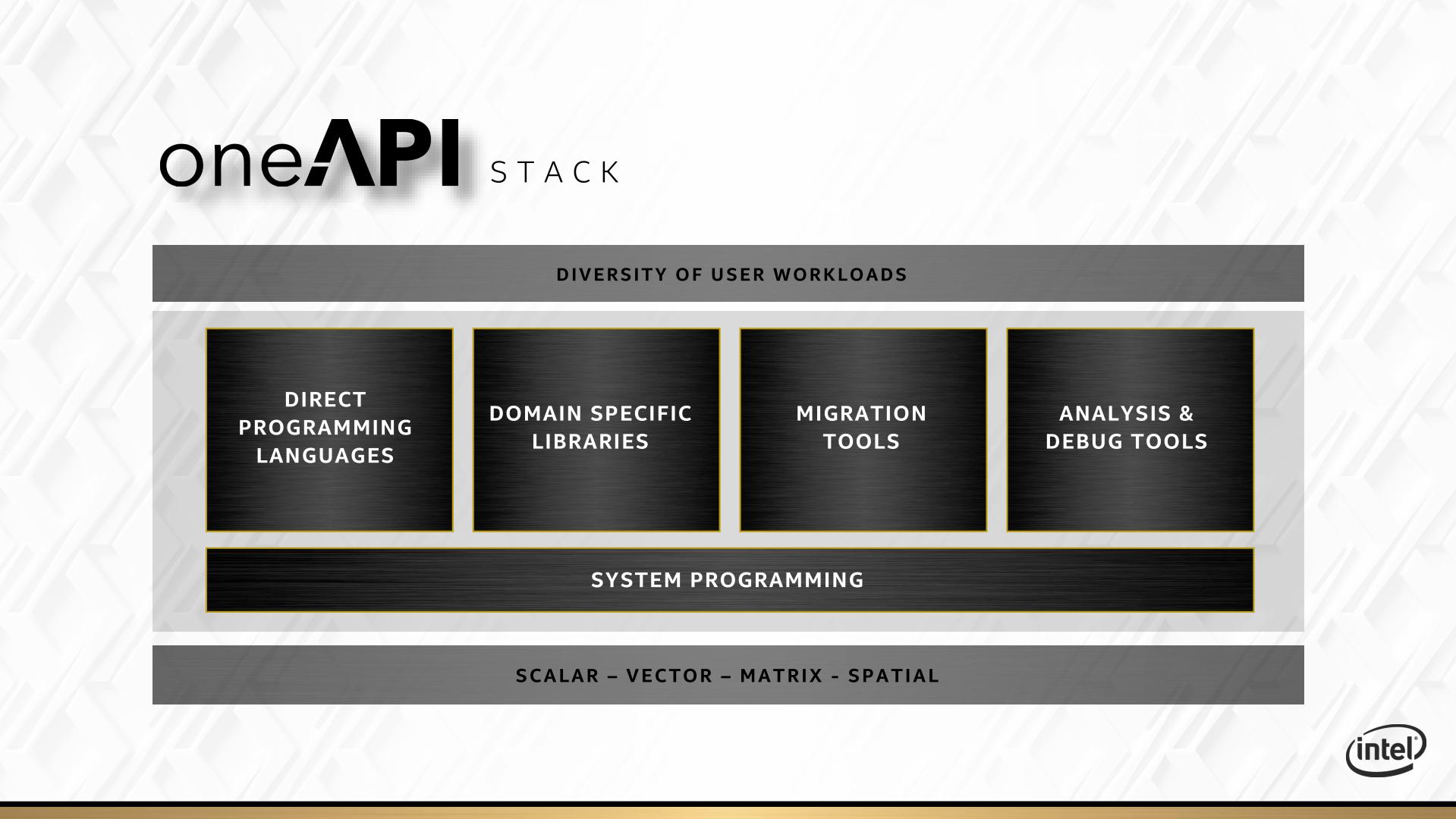
The underlying area that covers the rest is system programming. This includes scheduler management, peer-to-peer communications, device and memory management, but also trace and debug tools. The latter of which will appear in its own context as well.
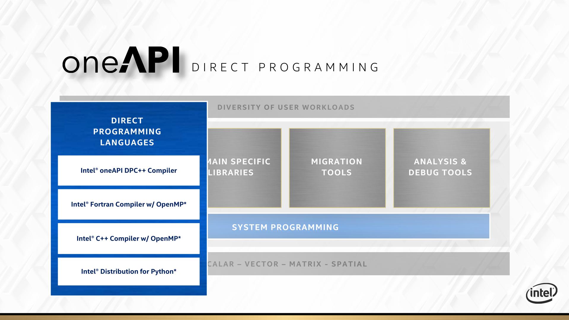
For direct programming languages, Intel is leaning heavily on its ‘Distributed Parallel C++’ standard, or DPC++. This is going to be the main language that it encourages people to use if they want portable code over all different types of hardware that oneAPI is going to cover. DPC++ is an intrinsic mix of C++ and SYCL, with Intel in charge of where that goes.
But not everyone is going to want to re-write their code in a new programming paradigm. To that end, Intel is also working to build a Fortran with OpenMP compiler, a standard C++ with OpenMP compiler, and a python distribution network that also works with the rest of oneAPI.
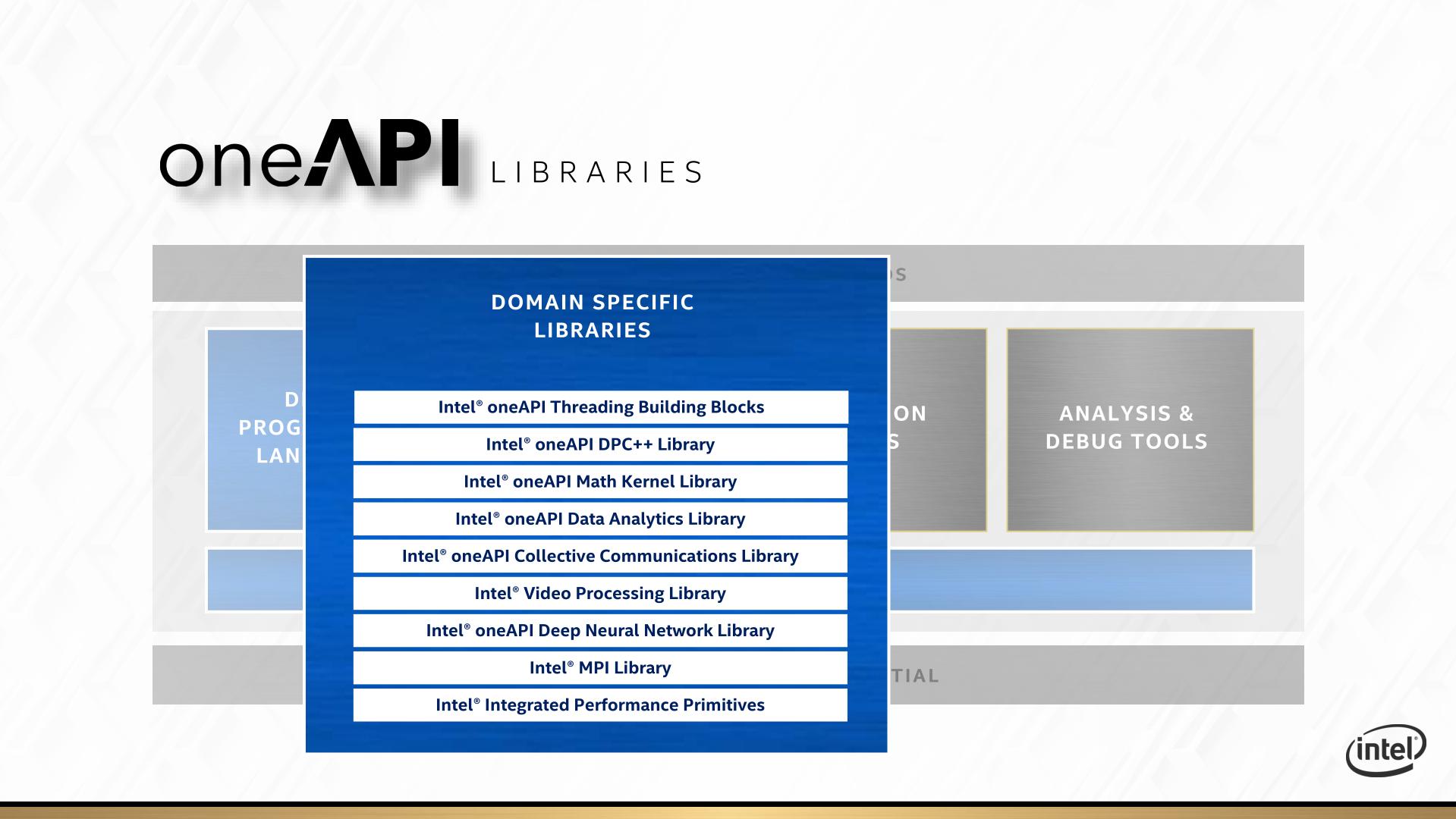
For anyone with a categorically popular workload, Intel is going to direct you to its library of libraries. Most of these users will have heard of before, such as the Intel Math Kernel Library (MKL) or the MPI libraries. What Intel is doing here is refactoring its most popular libraries specifically for oneAPI, so all the hooks needed for hardware targets are present and accounted for. It’s worth noting that these libraries, like their non oneAPI counterparts, are likely to be sold on a licencing model.
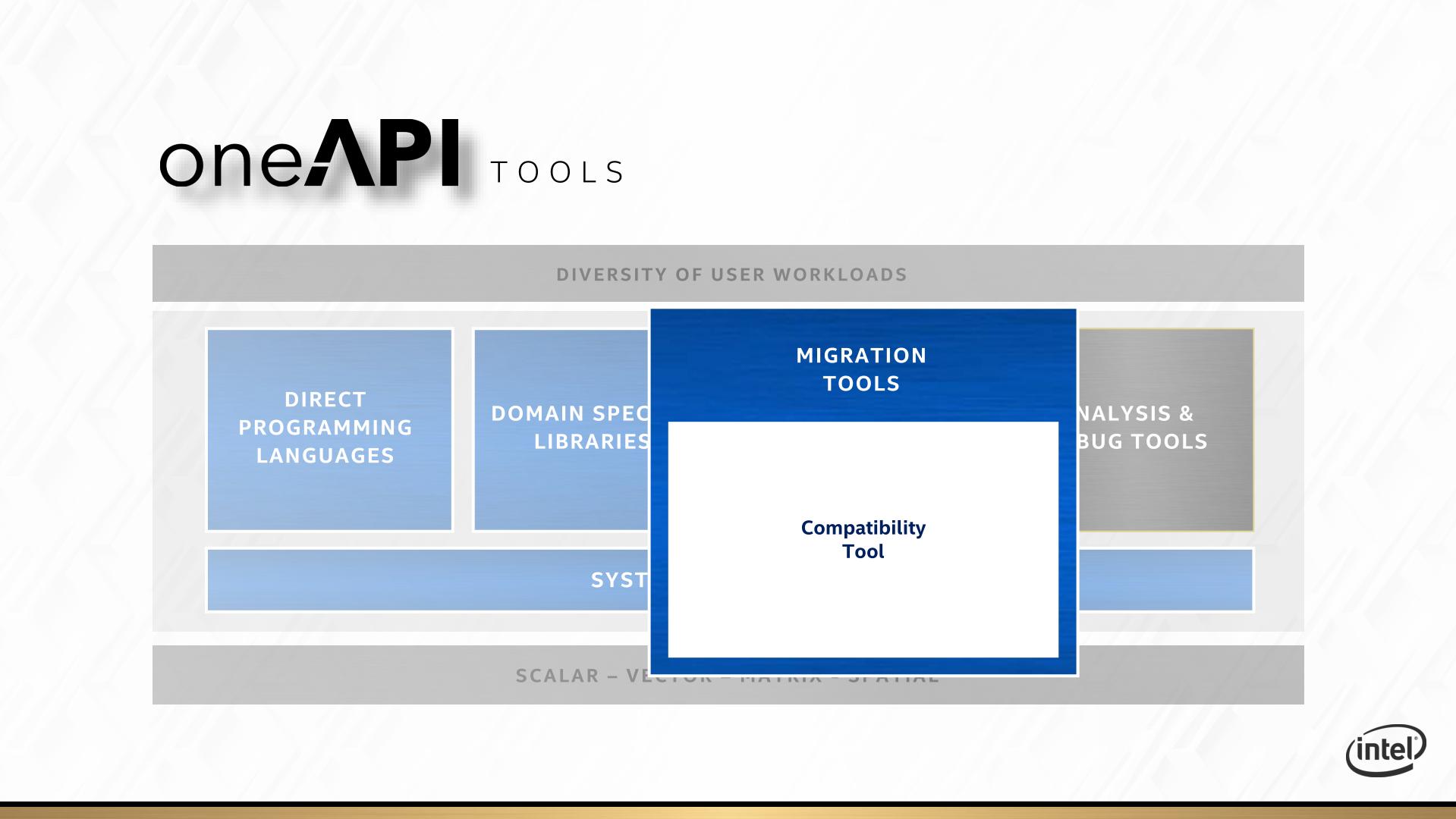
One big element to oneAPI is going to be migration tools. Intel has made a big deal what they want to be able to support CUDA translation to Intel hardware. If that sounds familiar, it’s because Raja Koduri already tried to do that with HIP at AMD. The HIP tool works well in some cases, although in almost all instances it still requires adjustment to the code to get something in CUDA to work on AMD. When we asked Raja about what he learned about previous conversion tools and what makes it different for Intel, Raja said that the issue is when code written for a wide vector machine gets moved to a narrower vector machine, which was AMD’s main issue. With Xe, the nature of the variable vector width means that oneAPI shouldn’t have as many issues translating CUDA to Xe in that instance. Time will tell, for obvious reasons. If Intel wants to be big in HPC, that’s the one trick they’ll need to execute on.
The final internal pillar of oneAPI are the analysis and debug tools. Popular products like vTune and Trace Analyzer will be getting the oneAPI overhaul so they can integrate more easily for a variety of hardware and code paths.
At the Intel HPC Developer Conference, Intel announced that the first version of the public beta is now available. Interested parties can start to use it, and Intel is interested in feedback.
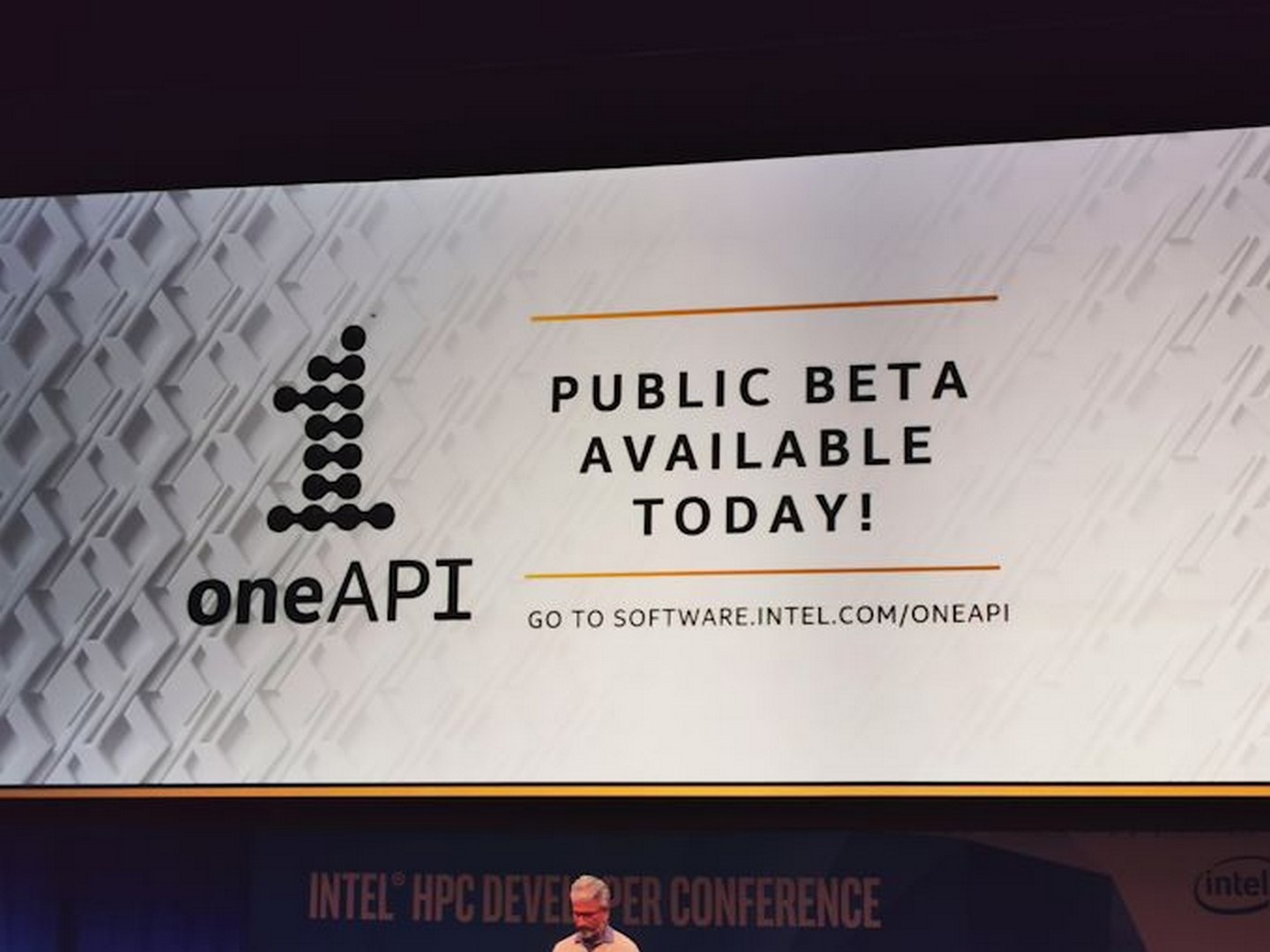
The other angle to Intel’s oneAPI strategy is supporting it with its DevCloud platform. This allows users to have access to oneAPI tools without needing the hardware or installing the software. Intel stated that they aim to provide a wide variety of hardware on DevCloud such that potential users who are interested in specific hardware but are unsure what works best for them will be able to try it out before making a purchasing decision. DevCloud with the oneAPI beta is also now available.
The First Xe-HPC Deployment: Aurora, with Xe Link
Some of this analysis is taken from our original Aurora Xe news post, but now with Xe Link information.
If you’ve skipped to this final page, it’s worth reading the last few. We’ve covered in detail what we can derive from Intel slides about the Xe architecture, the new Xe-HPC hardware paradigm, the Ponte Vecchio GPU in as much detail as we could figure out, and the new software strategy. All this page talks about is the major commercial deployment of Xe-HPC in a supercomputer: Aurora. If you want the juicy details on the hardware, and what we might see on the graphics side, take a read of the previous pages.
Aurora: Exascale in the USA
Part of the announcement at HPC DevCon was about the first deployment of Ponte Vecchio, to the new Aurora supercomputer for the Department of Energy at Argonne National Laboratories. Intel disclosed that it will be delivering Aurora in 2021, featuring two new future CPUs as well as six GPUs per node.
Intel has been working on the Aurora contract for a while now, and the project has changed scope over time due to market changes and hardware setbacks. Initially announced several years ago as a ‘deliver by 2020’ project between Argonne, Cray, and Intel, the hardware was set to be built around Intel’s Xeon Phi platform, providing high-throughput acceleration though Intel's AVX-512 instructions and the 10nm Knights Hill accelerator. This announcement was made before the recent revolution in AI acceleration, as well as Intel subsequently killing off the Xeon Phi platform after adding AVX-512 to its server processors (with the last breath Knights Mill receiving a very brief lifespan). Intel had to go back to the drawing board, and since Xeon Phi was scrapped, Intel’s audience has been questioning what it will bring to Aurora, and until today the company had only said that it would be built from a combination of Xeon CPUs and XeHPC GPUs.
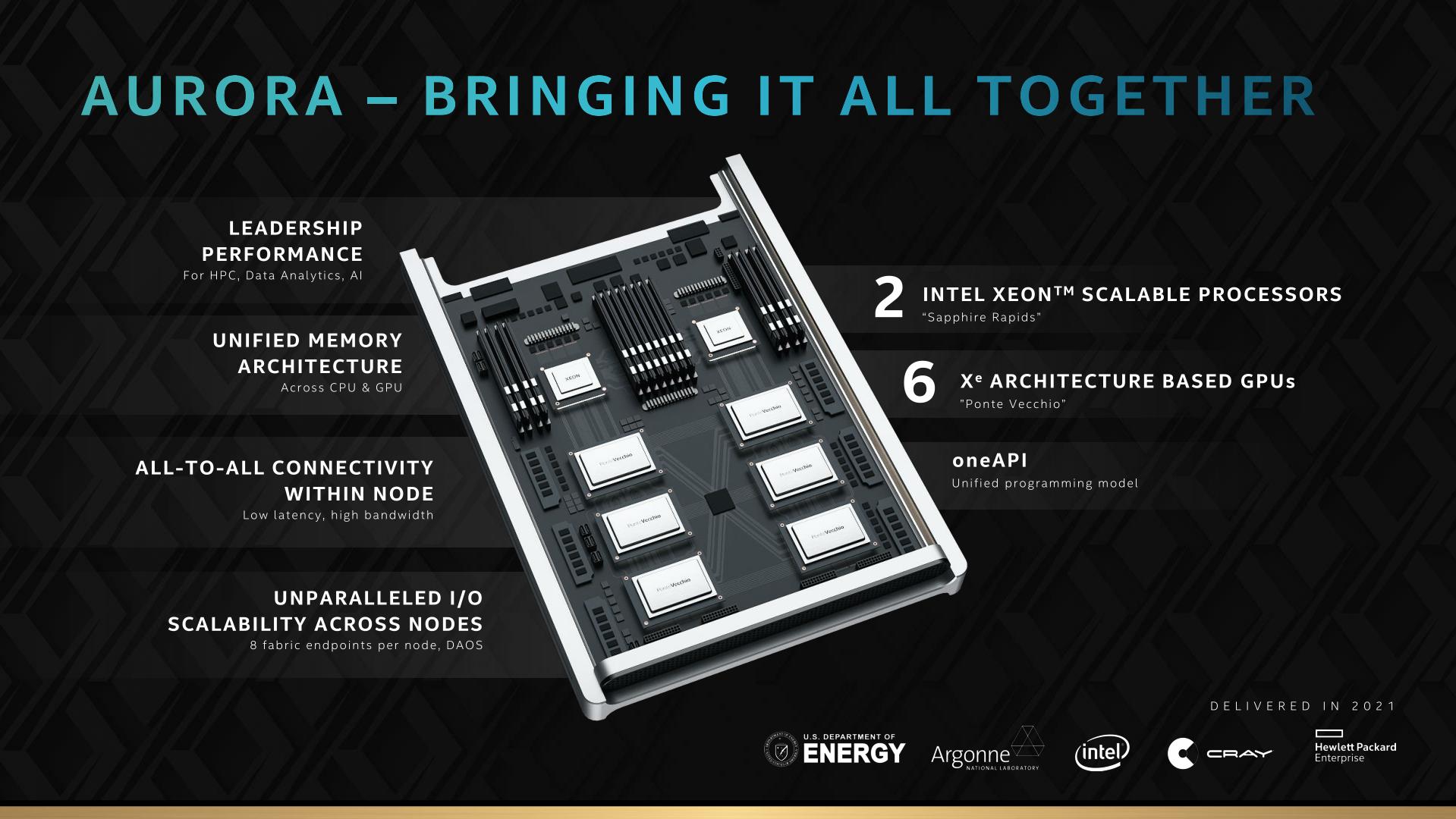
The two CPUs will be ‘Sapphire Rapids’ Xeon CPUs, which if you follow Intel’s release schedule, is the CPU after the CPU after the CPU after the one currently on the market. It goes Skylake, Cascade Lake (currently out), Cooper Lake (2019/2020), Ice Lake (2H2020), Sapphire Rapids (2021). The promise is that these CPUs will be on 10nm, and judging by the diagram will have 8 channels of memory (likely DDR5, but not confirmed). Sapphire Rapids are predicted to be Intel’s first enterprise CPUs to support the new CXL standard, which would also mean PCIe 5.0 support at a minimum.
With the two CPUs are six Ponte Vecchio GPUs. Judging by the diagram, it must be pretty obvious that these are not PCIe cards, but likely to be OAM or SXM2 modules, or whatever the newest standard will be at the time. Each GPU will be able to communicate directly to each other via CXL, which is an interesting element to the discussion. On these diagrams is a small black chip in the middle, which Intel announced as its new Xe Link chip.
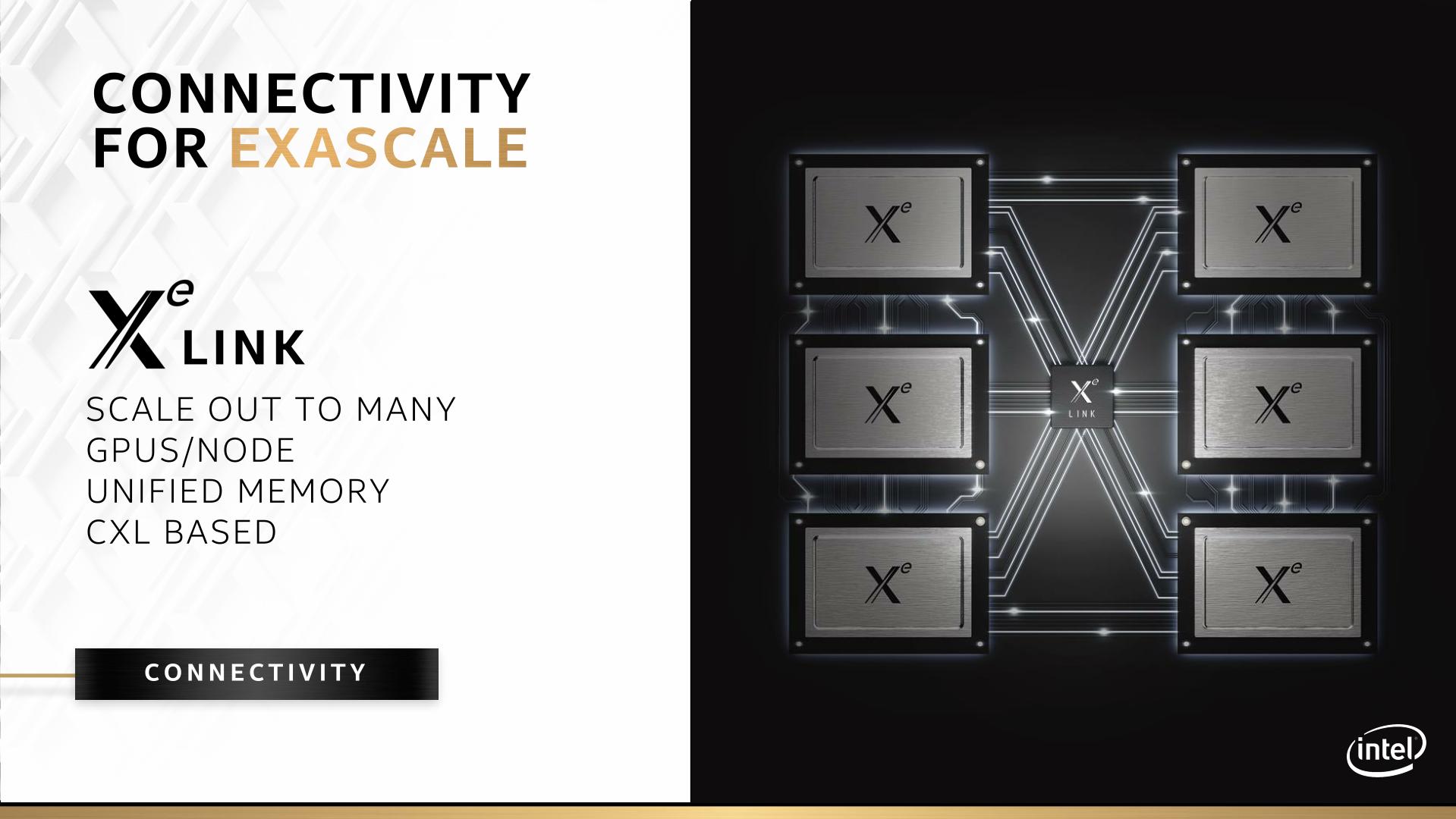
Much like NVIDIA’s NVSwitch, it looks like the Xe Link chip is there to mediate communications between all the GPUs in a node, and by what Intel says on this slide, between nodes as well. It would appear to also manage the unified memory of the system, and like the GPUs, it is CXL based. Part of the announcement on the links between the GPUs is that it should be an all-to-all design, despite the image above showing some GPUs communicating directly to each other and some only through the Link chip. We confirmed that this representation was inaccurate.
The CPUs will be Sapphire Rapids CPUs, Intel’s second generation of 10nm server processors coming after the Ice Lake Xeons. The announcement today reaffirmed that Sapphire Rapids is a 2021 processor; and likely a late 2021 processor, as the company also confirmed that Ice Lake will have its volume ramp through late 2020. Judging from Intel's images, Sapphire Rapids is set to have eight memory channels per processor, with enough I/O to connect to three GPUs. Within an Aurora node, two of these Sapphire Rapids CPUs will be paired together, and support the next generation of Intel Optane DC Persistent Memory (2nd Gen Optane DCPMM). We already know from other sources that Sapphire Rapids is likely to be DDR5 as well, although I don't believe Intel has said that outright at this point.
On the GPU side, all six of the GPUs per node will be Intel’s new 7nm Ponte Vecchio Xe GPU.
Each Aurora node will have 8 fabric endpoints, giving plenty of topology connectivity options. And with the system being built in part by Cray, connecting the systems will be a version of their Slingshot networking architecture, which is also being used for the other early-2020s US supercomputers. Intel has stated that Slingshot will connect ~200 racks for Aurora, featuring a total of 10 petabytes of Memory and 230 petabytes of Storage.
Guessing Ponte Vecchio Performance
With this information, if we spitball some numbers on performance, here's what we end up with:
- Going with Intel's number of 200 racks
- Assume each rack is a standard 42U,
- Each Aurora node is a standard 2U,
- We know the system has 200 racks.
- Take out 6U per rack for networking and support,
- Take out 1/3 of the racks for storage and other systems
- We get a rounded value of 2400 total Aurora nodes (2394 based on assumptions).
This means we get just south of 5000 Sapphire Rapids CPUs and 15000 Ponte Vecchio GPUs for the whole of Aurora. Now when calculating the total performance of a supercomputer, the CPU and Accelerator performance often depends on the workload required. If Ponte Vecchio is truly an exascale class GPU, then let’s assume that the GPUs are where the compute is. If we divide 1 ExaFLOPs by 15000 units, we’re looking at 66.6 TeraFLOPs per GPU. Current GPUs will do in the region of 14 TF on FP32, so we could assume that Intel is looking at a ~5x increase in per-GPU performance by 2021/2022 for HPC. Of course, this says nothing about power consumption, and if we were to do the same math at 4U per node, then it would be ~7500 GPUs, and we would need 135 TF per GPU to reach exascale.
Delivering The Hardware
Despite initially being a ‘deliver by 2020’ project, Intel is now saying that Aurora will be delivered in 2021. This means that Intel has to execute on the following:
- Manufacturing at 10++ in sufficient yield with respect to cores/frequencies
- Manufacturing at 7nm for chiplets, both in yield and frequencies
- Transition through DDR3 to DDR4 (and DDR5?) in that time frame
- Transition through PCIe 3.0 to PCIe 4.0 and PCIe 5.0 in that time frame
- Release and detail its 2nd generation Optane DC Persistent Memory
- Provide an SDK to deal with all of the above
- Teach researchers to use it
On those last two points, Intel has stated that Ponte Vecchio and Aurora will be a primary beneficiary of the company’s new OneAPI SDK. This industry initiative, spearheaded by Intel, is designed to use a singular cross-architecture language called ‘Data Parallel C++’, based on C++ and SYCL, that can pull libraries designed to speak to various elements of Intel’s hardware chain. The idea is that software designs can write the code once, link appropriate libraries, and then cross-compile for different Intel hardware targets. In Intel’s parlance, this is the ‘xPU’ strategy, covering CPU, GPU, FPGA, and other accelerators. Aside from Argonne/Cray, Intel is citing Lenovo and Atos as key partners in the OneAPI strategy.

In order to achieve a single exascale machine, you need several things. First is hardware – the higher performance a single unit of hardware, the fewer you need and the less infrastructure you need. Second is infrastructure, and being able to support such a large machine. Third is the right problem that doesn’t fall afoul of Amdahl’s Law – something that is so embarrassingly parallel that can be spread across all the hardware in the system is a HPC scientist dream. Finally, you need money. Buckets of it.
In the past few years, the top supercomputers in the world have addressed all of these requirements by orders of magnitude: hardware is faster, infrastructure is readily available, traditionally serial problems are being re-architected to be parallel (or lower precision), and governments are spending more than ever for single supercomputers. A $5 million supercomputer used to get a research group into the top echelons of the Top 500 list. Now it’s more like $150+ million. The current leader, Summit, had an estimated build cost of $200 million. And Aurora will handily top that, with the deal valued at more than $500 million.
When I asked before the announcement if Argonne would be the first customer of Ponte Vecchio, the Intel executive heading the briefing dodged the question by instead answering his own, saying ‘we’re not disclosing other customers’. In all my time as a journalist, I don’t think I’ve ever had a question unanswered and dodged in such a way. Unfortunately I had no opportunity in the open Q&A session to follow up.
Ultimately, based on what we know so far, Intel still has a lot of work to do to deliver this by 2021. It may be the case that Aurora is that culmination of all its technologies, and that Intel would be prepared to use the opportunity to help smooth out any issues that might arise. At any rate, some of these technologies might not get in the hands of the rest of us until 2022.
Hopefully, when Aurora is up and running, we’ll get a chance to take a look. Watch this space.


