Original Link: https://www.anandtech.com/show/14769/hot-chips-31-live-blogs-intel-10nm-spring-crest-nnpi-inference-chip
Hot Chips 31 Live Blogs: Intel 10nm Spring Hill NNP-I Inference Chip
by Dr. Ian Cutress on August 20, 2019 2:55 PM EST
03:35PM EDT - .
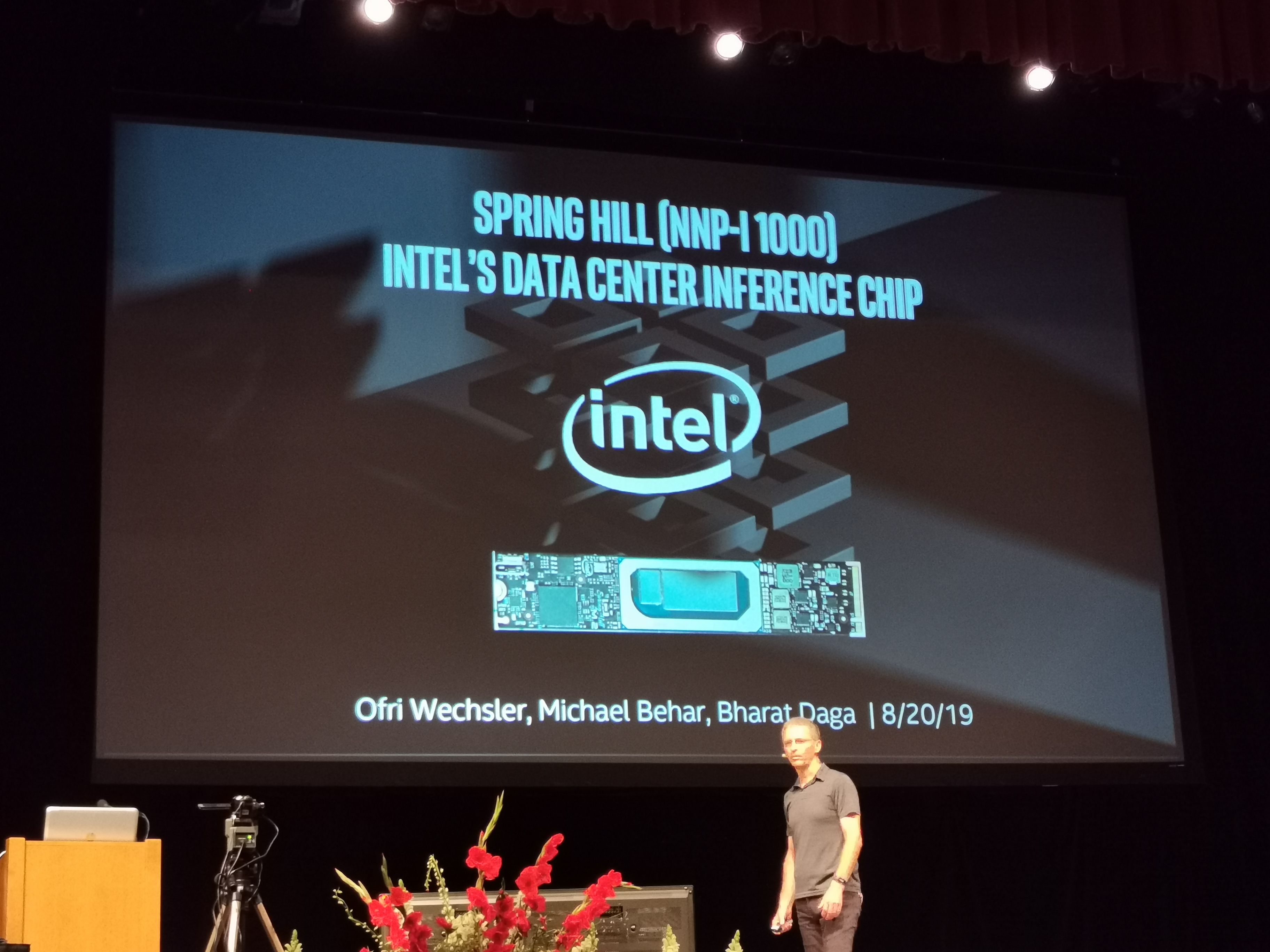
03:05PM EDT - One of Intel's future 10nm products is the Spring Hill NNP-I 1000 Inference Engine. Today the company is lifting the lid on some of the architecture behind the chip.
03:05PM EDT - This is a 10nm chip !
03:05PM EDT - More info coming. I've been briefed on this
03:06PM EDT - Haven't had time to write it up yet. But here's the live blog
03:07PM EDT - The importance of machine learning and inference
03:07PM EDT - chip architecture becomes important
03:09PM EDT - Purely internal Intel chip
03:09PM EDT - Comes in M.2 form factor and a custom form factor
03:10PM EDT - M.2 module shown comes with 16 GB DRAM onboard
03:10PM EDT - 5 minutes in and still on the intro slide
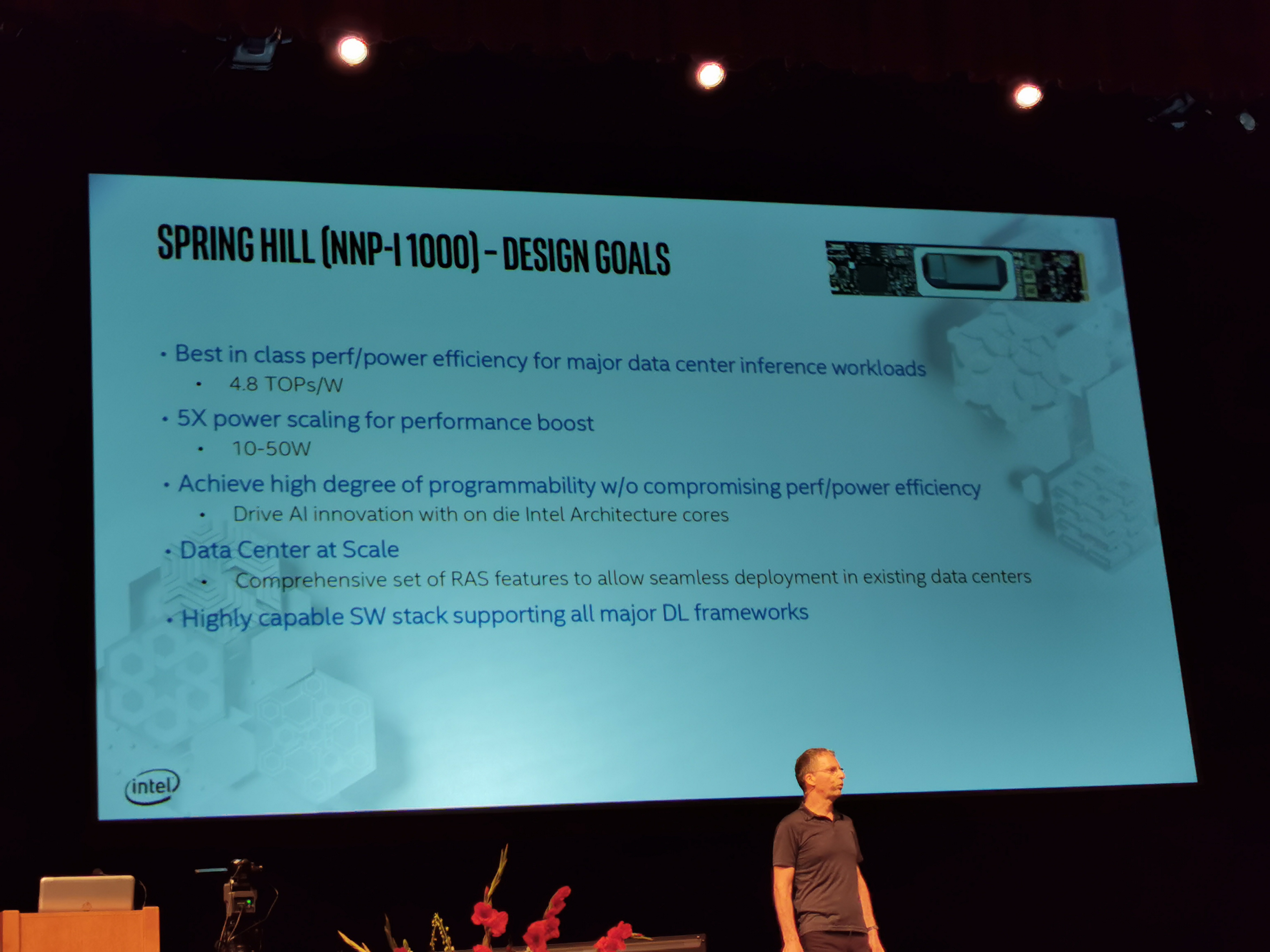
03:11PM EDT - Up to 4.8 TOPs/W
03:11PM EDT - Same silicon can go 10W to 50W
03:11PM EDT - This is a DC chip
03:11PM EDT - Contains Intel Sunny Cove cores
03:11PM EDT - Highly capable SW stack supporting all major DL frameworks
03:11PM EDT - Having Sunny Cove means AVX-512 onboard
03:14PM EDT - RAS features for DC
03:15PM EDT - Still on this slide
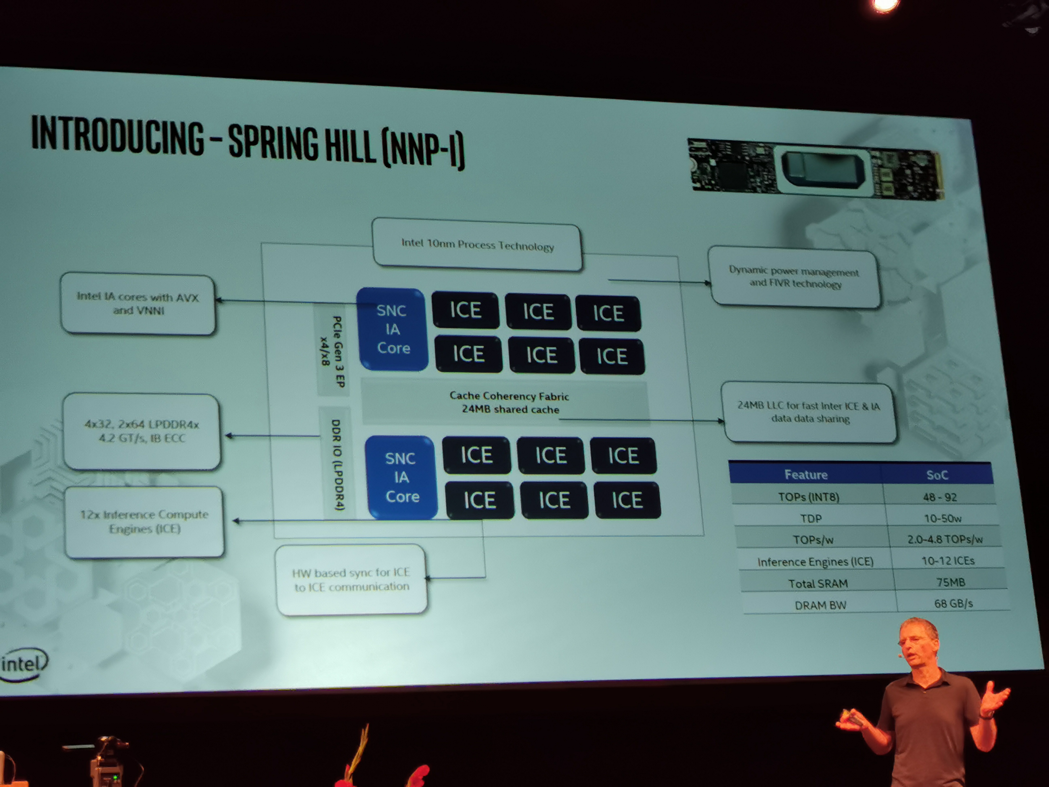
03:16PM EDT - 2 Sunny Cove Cores, 12 Inference cores, 24 MB shared cache
03:16PM EDT - 'ICE'. But not ICE lake
03:16PM EDT - It's basically an 8-core Ice Lake chip with the graphics and 6 cores removed, and ICEs moved in
03:17PM EDT - Same DRAM support as Ice Lake
03:18PM EDT - Each of the Sunny Cove cores can control any of the 12 ICE cores
03:18PM EDT - PCIe 3.0 x4/x8 connection to the host CPU
03:18PM EDT - 75MB total SRAM, 68 GB/s DRAM BW
03:19PM EDT - 10+ process node
03:19PM EDT - Designed for other power constrained problems
03:19PM EDT - Power management same as Ice Like
03:19PM EDT - Lake
03:20PM EDT - Map workloads to allocated power budgets
03:20PM EDT - Standard PCIe device
03:21PM EDT - In 50W mode, it's obviously not an M.2 drive
03:22PM EDT - Each ICE can do 4K MAC/cycle
03:23PM EDT - Supports FP16 / INT8/4/2/1
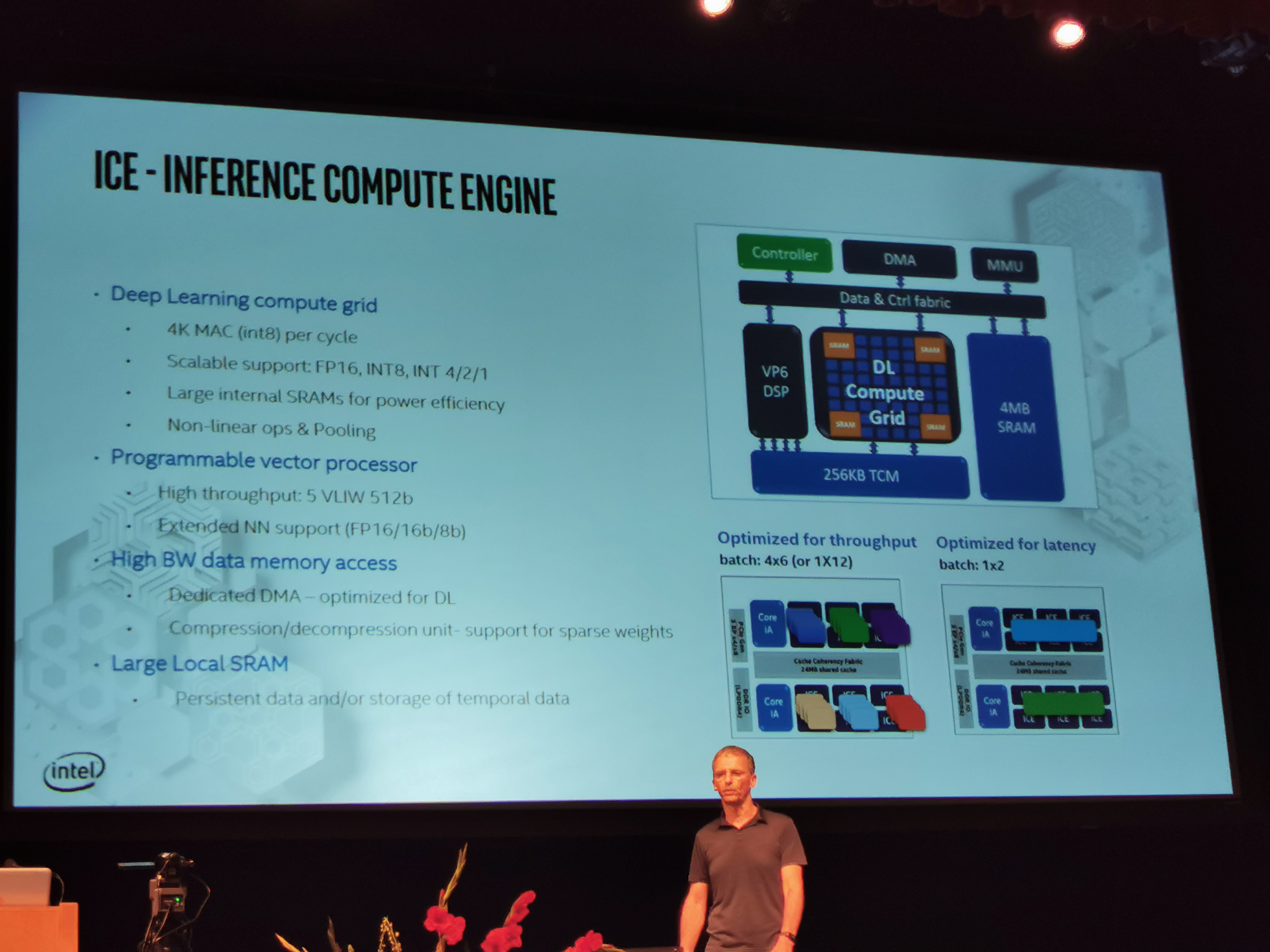
03:23PM EDT - Dedicated DMA optimized for DL
03:23PM EDT - Compression/decompression unit for sparse
03:24PM EDT - 4MB SRAM per ICE with 256KB TCM between Compute Grid/Vector DSP
03:24PM EDT - Tensilica V6 DSP per ICE

03:25PM EDT - DL Compute Engine looks like a 4D grid
03:25PM EDT - 5D Stride DMA
03:25PM EDT - Post-processing op-fusion
03:26PM EDT - Minimize data transfer
03:26PM EDT - Non Linear Maxpool ElementWise Controller
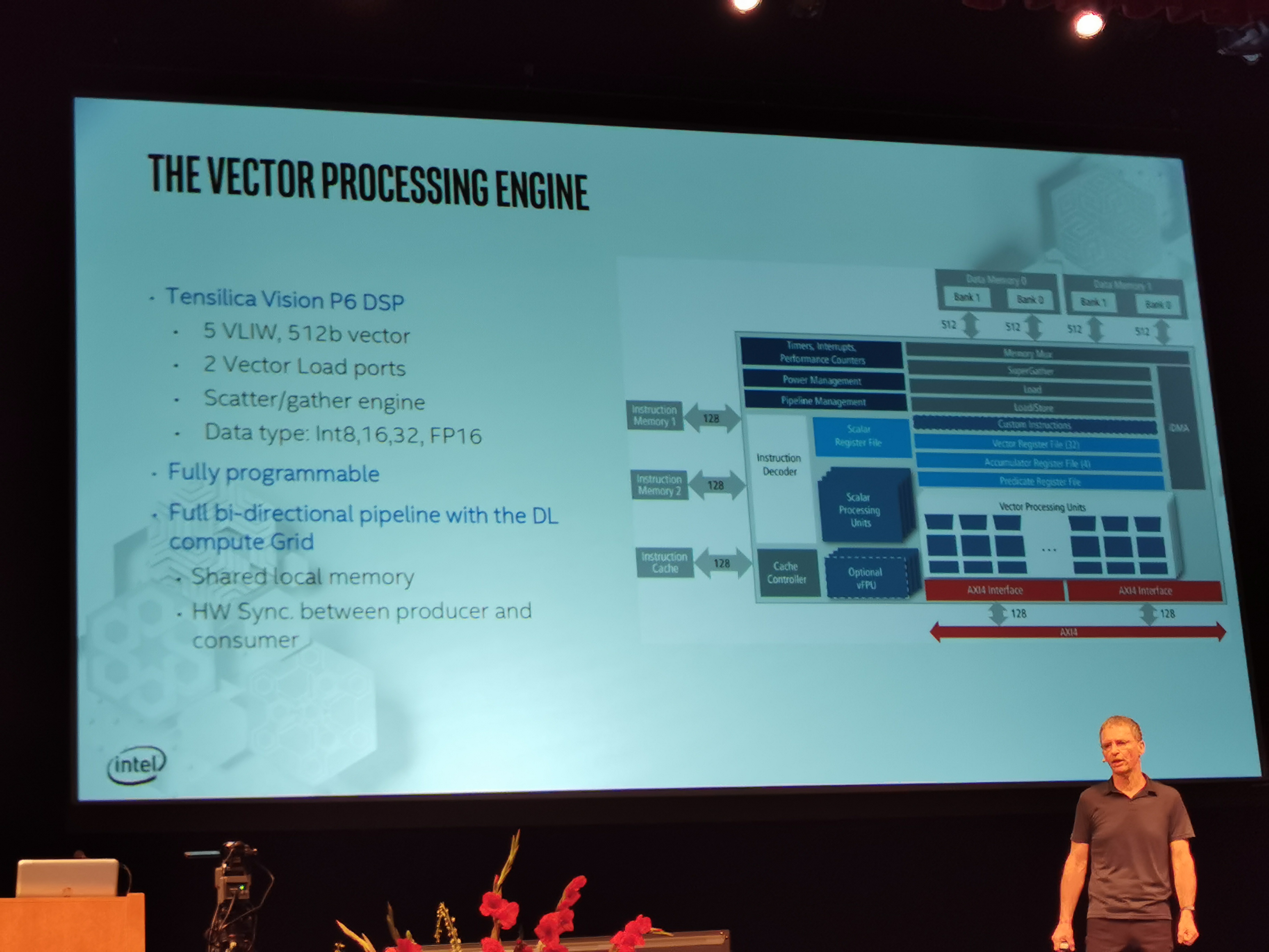
03:28PM EDT - DSP has 2 vector load ports, supports native scatter/gather engine
03:28PM EDT - Fully programmable
03:28PM EDT - bi-directional pipeline with the DL compute grid with shared local memory and hardware sync
03:28PM EDT - 4 levels of memory

03:29PM EDT - It's like an 8-core Ice with the Cores ripped out with 2 ICEs put in
03:29PM EDT - Up to 32 GB of DRAM
03:29PM EDT - No BF16 support
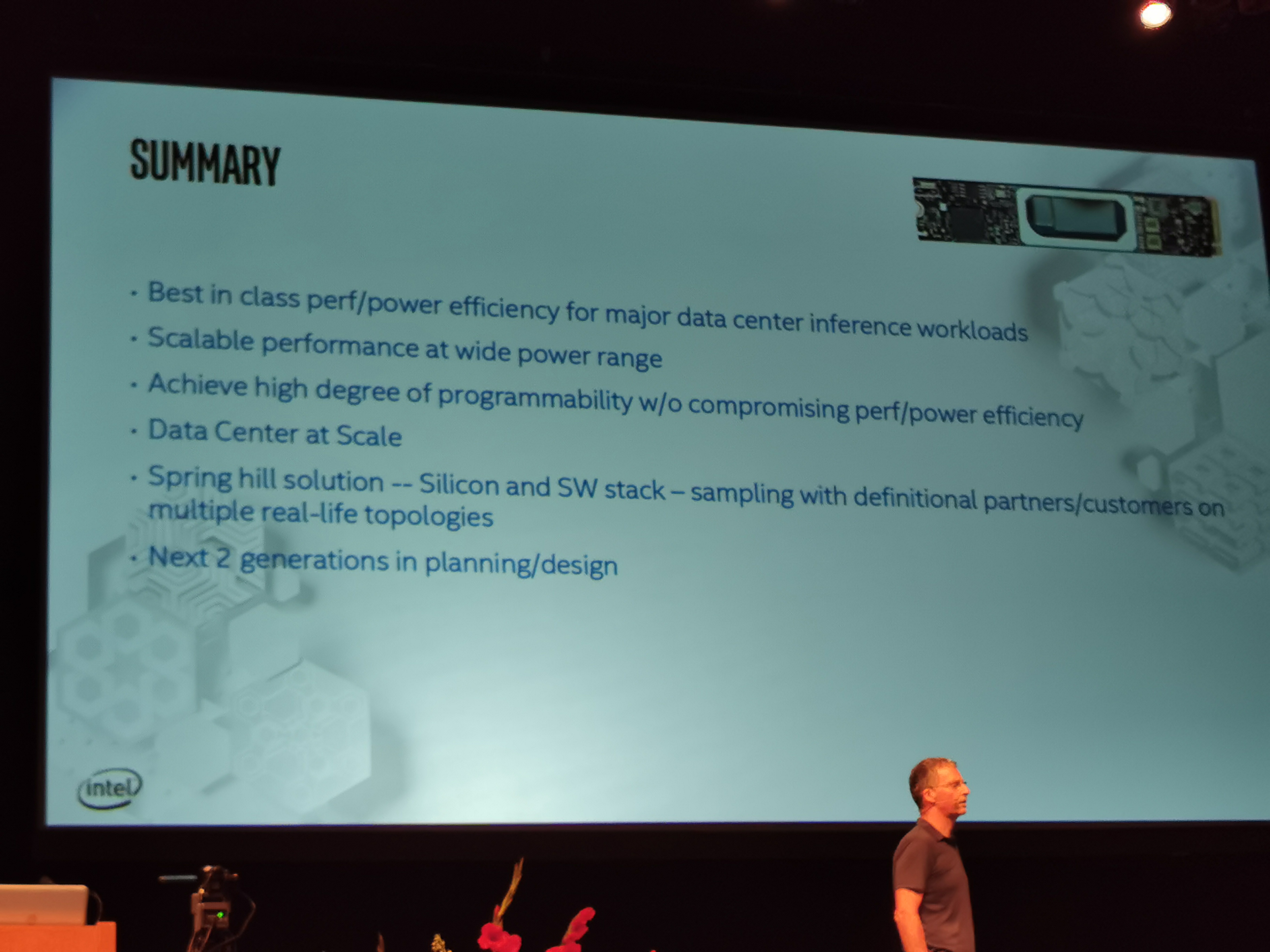
03:30PM EDT - ResNet-50, 3600 Inferences per second at 10W
03:31PM EDT - Going form 2 to 12 cores gives 5.85x speedup
03:35PM EDT - That's a wrap. Time for lunch. Next up is TSMC Keynote at 1:45pm PT.


